


SkyVision BOX-800 VGA to TV converter
This documents describes how SkyVision BOX-800 video converter works. This document is ment to describe the operation of one commercial VGA to TV converter product. This text is written and graphics are drawn by Tomi Engdahl. The information for this text is taken from Jere M�kel�'s Master's Thesis "Software Design for a video conversion equipment" (Helsinki University of Technology, 1994, 69 pages).
Introduction
SkyVision is a Finnish company which makes video conversion products. Their computer to TV products are BOX-800 VIDEO CONVERTER (small external Video Converter, which converts PC/MAC images to PAL/NTSC video) and VGA/PAL Card (PC add-on-card which plugs to VGA card feature connector and supports resolutions up to 640x480 with 256 colors).
Jere M�kel� made his Masters Thesis about SkyVision BOX-800 software design at 1994 to Helsinki University of Technology Computer Technology lab. This documents is written based on this Masters Thesis. I have added some of my own notes to the text (notes start with NOTE:).
Technical specifications of the BOX-800 converter
- Supports VGA resolutions up to 800x600 resolutions
- Supports Macintosh resolutions up to 640x480
- Number of colors supported 32K colours (5 bits ber RGB component)
- Built-in flicker fixel filters
- Picture scaling options
- External video converter box with front-panel controls
- RGB, composite and S-VHS outputs
Earlier solution used by SkyVision
SkyVision has manufactured and sold a VGA to TV converter card which plugs to the ISA bus. That card takes the vidoe data from VGA card feature connector in digital format. The converter card takes the VGA palette information, reset signal and power form the ISA BUS. Because the palette IC in the converter card is at the same I/O address as the VGA card palette chip then all writes to VGA palette chip also go the the converter card palette chip (NOTE: this works only if both the VGA card and the converter card are plugged to ISA bus). This card support all VGA display modes up to 640x480 resolutions with up to 256 with refresh rates up to 72 Hz (NOTE: VGA feature connector limits the the number of colors to 256 and also available resolution). This converter card has RGB (SCART connector), composite vidoe and super-VHS outputs.
This converter works using the following conversion method:
- VGA scanlines are routed to memory buffer in the converter card
- the picture data is then read from the memory according the TB standard
- The memory consists of two blocks to support interlaced TV picture easily (one block stores even lines and one odd lines)
- VGA lines are stored to memory block so that first TV field can be read frrm first memory block and second TV field can be read from second memory block
- Both memory block use FIFO type memory which allows separate input and output clocks to be used
- Memory also includes reset to beginning to each VGA and TV field
- Need for memory is limited by only storing the active parts of active VGA scanlines
- The difference in the number of TV lines and VGA lines is solved by storing selected VGA scanlines twice to the buffer memory
- Flicker in Tv picture is reduced by averaging two scanlines in the output
- The controlling of the whole system is done using FPGA style ASIC IC
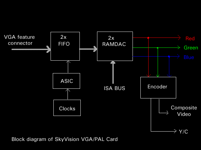
(NOTE: This same block diagram applies quite much to other similar comverters in the market at the same time)
Advances in the market demand new products
When graphics application became more common in PCs the PC graphics displays started to use higher resolutions and new refresh rates. New grpahics display modes which were introduced quite quicly to wide use were 800x600 (56.25, 60 and 72 Hz) and 1024x768 with and without interlacing. PC computers started to use faster busses (EISA, MCA, VLB and later PCI) for interfacing cards. Eve increasing need for multimedia applications started to increase the need for VGA to PAL converters which support those.
(NOTE: Graphics card with highcolor (15bit (32K) and 16 bit (64K) colors) and truecolor (24bit (16.7M)) became also available. The limitations of VGA feature connector bandwidth and implementation caused that those high resolutions could not be transferred though the old VGA feature bus. When graphics cards move to other busses the converter card sitting in ISA BUS could not anymore get the palette data sent to VGA card).
Different VGA/PAL converter makers tried the meet the new market demands using following methods:
- Converters are implemented as external conversion boxes which connect to analogue VGA monitor connector of the VGA card (this enabled also those converters to be connected to for example to Apple Macintosh computers)
- Converters start to support new higher graphics resolutions (some scaling is needed to make them to fit to TV screen resolution which is 575 lines in PAL standard)
- Some converters started to offer Genlock and Video Overlay functions
- The number of colors has to be added to support new graphics modes with higher number of colors
Support of higher resolutions need some scaling to be done because all VGA scanlines can't be displayed in TV screen. For example when 800x600 mode is converted to 572 lines PAL format then at least 25 VGA scanlines must be left out. If the scanlines are left out at constant distribution over the VGA screen area then then the picture quality stays quite propably adequate. If 1024x768 mode needs to be shown in TV screen then at least 193 scanlines must be removed (around 25% of VGA screen scanlines). Even more scanlines must be left out in NTSC TV standard (NOTE: NTSC has 484 active scanlines). The scaling cna be just done by leaving out those scanlines but better results can be made using digital filtering (there are chips for this but those were expensive and hard to get at 1994).
What users wanted from new product ?
SkyVision made a market research what users wanted from new product: Users wanted to have an external conversion box because card versions can't be used with portable PCs and external device is more easily portable. New high resolutions needs to be supported. Users wanted a possibility to scale the picture size in vertical and horizontal directions. There was need for better flicker reduction filters and possibility to choose between different filtering methods (NOTE: different applications need different filters, filtering is usually tradeoff between the efectiveness of filtering and the picture accuracy).
The existing vidoe conversion cards and other equipments at 1994 were priced between 2000 and 15000 Finnish marks (around 500-3000 US dollars). The cheapest products had typically poor picture quality and problem with screen mode support. Many converters needed software drivers which kept the VGA screen refresh rate constant. Components and application notes for this kind of simple converters vere already available. If Finnish quite small scale product needs to compete with those the inexpensive converters is must have some unique features which other products can't provide (for example using own ASIC chips to solve problems where there are ready made ICs available).
Needed specifications for new product:
- The converter must be an external box
- The converter must have a Genlock option to make it possible to sync it to video studio equipments
- For advanced used the converter includes vidoe overlay option
- Converter must support screen resolutions up to 800x600 resolutions
- New higher screen refresh rates (up to 72 Hz) must be supported
- Converter should also support Apple Macintosh at 640x480 resolution, new connector for Macintosh must be added because different monitor control signals are used
- The picture in TV must be adjustable like the picture in computer screen
- Better flicker reduction filtering must be used in the new product
- Converter uses external +9V power supply to avoid safety type approvals
- Horizonal and vertical picture size adjustments (potentiometers)
- Horizonal and vertical picture position adjustments (potentiometers)
- Switch to select the flicker reduction filter operation
- Switch which makes to do "freeze frame"
- Switch to select TV-standard: PAL or NTSC
- +9V power input
- Composite video output
- S-VHS output
- RGB output
- Genlock input
- VGA monitor signal input connector
- Apple Macintosh monitor input connector
Converter achitechture
VGA input implementation
The input connector for converte is input connector which accepts the video signal from VGA card. The VGA signal input in the converter is high impedance which enables the original VGA monitor to be also connected with the converter (the converter cable has connectors also for VGA card and original VGA monitor, te high impedance converter input does not affect the picture quality). Sync signals are sent to the converter separately (hsync and vsync) as VGA standard says.VGA card needs always the ID bits so that the card can detect what type of monitor is attaced to the card. Because the converter must also be used without monitor the converter has a logic to generate the necessary monitor identification bits to VGA card (and VGA card always sees monitor attaced).
Video conversion impelementation
The block diagram below describes the main blocks of the SkyVision BOX-800 VGA to TV converter:
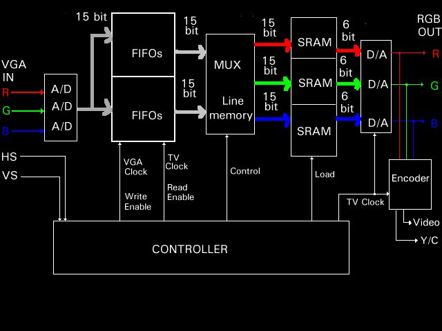
There is a separate 5-bit parallel A/D converter for each color component to convert the analogue VGA video signal to digital format which can be stored to buffer memory. 5 bits per resolution per color component makes it to be able to represent 32768 colors. The clock rate is made to be same as which the VGA card uses and can be up to 50 MHz. The clock is generated using programmeble clock generator IC which is programmed by the converter controlling microcontroller to match the clock frequency used in the detected VGA screen mode.
The results of A/D conversion are stored to field memories. The VGA data is stored to those memories at one page (two fields) at the time. Field memories are implemented using same FIFO memories as used in the previous video conversion card made by SkyVision.
The flicker filtering is implemented using SRAM filter block. The filtering is used separately for each RGB color component. For each filtering there are three pixels used (the pixel from the current pixel line which is being drawed and one from upper and lower scanlines). Those three pixel values can be read efficently by reading both field meories at the same time and using one scanline memory buffer. Three pixel values are used to make a 15 bit address to SRAM memory and the memory location contains the filtered pixel values (those tables are loaded by the controlling microcontroller when converter is started and filtering mode is changed, this takes less than 1 second). The contents of the SRAM memory determinen what kind of filtering is done and this allows impelementation of many different filtering methods. The filtering methods implemented with SRAM filter (n means scanline number and x(n) pixel value in scanline n in the equations):
- No filtering (used for photorealistic pictures etc.)
- Simple FIR filtering which uses three pixels values and sums them together using predefined weighting factors (out(n)=a*x(n)+b*x(n-1)+c*x(n-2))
- Two scanline averaging (out(n)=(x(n)+(n-1))/2)
- Non-interlaced output (data from only one field memory is used)
Controlling of the converter
A/D converter block needs a clock signal which has the same frequency as VGA card clock signal. For this the microntroller has to detect the active VGA mode and then program the frequency syntetizing chip to generate right clock frequency. The FIFO input block needs also that VGA clock signal and enabling signal whcih tells when the active part of the VGA frame is digitazed ans should be stored to the FIFO memory. Every time a new VGA frame is started (seen from vertical sync signal) the input memory address is reset to zero position.
The reading of picture data from FIFO memory is done using TV signal frequency clock and enable signal which tells when active part of picture is going on. Every time a new TV field is started (USG chip Vertical Drive signal) the read side address is reset to zero position.
In normal display operation the SRAM does not need any controlling or their contents does not need to be changed. When the content of SRAM memory needs to be changed (when filtering is changed) then the memories are discoonected from normal video conversion chain and are connected to the microprocessor though control logic which allows microprocessor to write data to them. When SRAM is disconnected from video conversion chain the video output is blanked because the SRAM outputs doer not at this time contain any valid video data.
D/A converter block is controlled using tha same TV output clock as the the FIFO reading. The video encoder IC needs also clolor subcarrier frequency and timimg signal.
THe controlling in this converter was implemented using an ASIC chip (3000 gate FPGA) and 80C31 microcontroller. Other chips in the converter controlling block are frequnecy syntetizer chip and Universal Syncronization Generator (USG). Frequnecy syntetizer chip generates VGA and TV clocks. Universal Syncronization Generator (USG) generates TV syncronization signals which are used by RGB output and video encoder. Universal Syncronization Generator chip generates the following signals which are used in this converter:
- TV Vertical Drive (tells when video frame starts)
- TV horizonal sync signal
- RGB output timing signals (syncronization signals)
- Timing needed by video encoder chip
ASIC chip handles the pixel frequency and parallel operating functions:
- VGA side syncronization and encoding controlling (clock, enable, new frame reset)
- TV side syncronization and encoding controlling (clock, enable, new frame reset)
- Processes horizonal and vertical sync signals for microcontroller (always same sync polarity)
- Helps microcontroller in VGA mode detection (detects between 350 and 400 line modes)
- Generate odd/even field control signal for SRAM filters using USG chip Vertical Drive signal
- Generates microcontroller clock
- Generates video encoder color subcarrier frequency
- Tells to microcontroller if PAL or NTSC signal is selected by user
- Reads front panel controls (buttons directly, potentiometers using 6-bit A/D chip connected to I2C bus)
- Controls the ASIC register values (picure horizonal and vertical position)
- Loads data to SRAM filter bank when needed
- Detects the VGA mode in use (ASIC supplies some processed signals)
- Programs Frequency syntetizer chip clock divider registers
- Programs Universal Sync Generator
- Selects to which frame memory the current VGA scanline is written (odd, even, both, not written at all) by writing this controlling information to ASIC control register every scanline before active part of scanline starts. This controlling is needed because in some screen modes some VGA lines must be discarded or or doubled to make the vertical resolution to match TV resolution. If Freeze function is activated no data is written to frame memories.
- Examines the monitor type bits sent by monitor and makes the converter to emulate monitor if real monitor is not connected (monitor ID bits, RGB signal high impedance/75 ohm termination controlling)
Detection of VGA mode
Microcontroller has to detect the VGA mode which is in use. ASIC chip preprocesses sync signals so that the microcontroller always receives sync signals at same polarity. VGA screen mode is detected by counting the number of scanlines in the screen mode and by measuring the vertical sync frequency of screen mode (measure frame time using timer). There are two VGA modes (350 and 400 line mode) which can't be detected as different modes using the sync signals only and the ASIC logic detect which one of those is in use when this is needed.
When VGA screen mode and TV output mode are detected the clock frequency syntetizer IC can be programmed to right frequencies.
Microcontroller program operation
Program timing:
- Wait for veritcal sync end
- Check if there is changes in operating environment and and wait for active
- Do the active scanline functions
- Microcontroller sync to horizonal sync start
- Write the control information to ASIC for next scanline and read the control information for scanline after that from microcontroller memory
Field memory controlling tables
Microcontroller memory has data table which tells which VGA scanlines are stored to which field memory. This table has two bit entries and each of them tells if the data is written to odd field, even field, both field or not written to memory at all. If the VGA screen has less lines than TV lines then some scanlines are copied to both fields. If VGA screen has more scanlines than TV picture then some scanlines from VGA frame are not written to field memories. In some cases the number on scanlines in VGA and TV screens match and the VGA picture can be directly transferred to field memories. For every vertical size setting, screen resolution and TV mode there is separate mapping table in the micrcontroller memory.
When line doubling or removing is done are at even distribution over the scanlines this should give a good picture on average. In windows screen a typical problem is one scanline wide lines in Window borders. Some of those lines can sometimes dissaperar totally from the displayed picture. This problem can be solved by slightly adjusting the picture size settings when the necessary scanline becomes visible.
Mapping the front panel to controls to converter settings
Vertical size values are mapped to avialable vertical size settings in that screen resolution and TV mode combination. TV picture vertical starts and end must be set according the displayed screen size and position.
Number of vertical pixels in the TV screen scanline is set to same as the number of horizonal pixels in active VGA screen scanline. When horizonal position or size is adjusted the scaline start and end register values are changed. This table is quite large because the values depend on horizonal settings and VGA screen resolution. The horizonal size position setting adjust the TV clock rate which makes the constant number of pixels to take different amount of scanline time. The settings for clock syntetizer registers are stored to the table (the optimal values are compiled using separate tools).
Improving the product
If the refresh rates become higher the microcpntroller has to be changed to a faster version. Using a faster microcontroller can lead to problems in I2C bus controlling.
If the resolution support is increared to higher resolutions than 800x600 the, method where some VGA scanlines are just removed is not good enough because considerable amount of scanlines (aroun 25% in 1024x768 resolution) must be removed and of those lines are just removed this causes unacceptable loss of picture quality. To solve this loss of information problem the resolution should be reduced using more advanced FIR filtering. In this product iw would need that the digital video scaling IC should be fitted before the frame buffer memory. If separate FIR filtering is used the SRAM filtering might not be mecessary to avoid flickering.
The original version of the product does not contain video overlay hardware. The circuit board has free space reserved for it to make adding it later possible without major modifications to the design.
Information sources
- Jere M�kel�, Software design for a video conversion equipment, Master's Thesis, Helsinki University of Technology, August 23, 1994, 69 pages
Tomi Engdahl <[email protected]>