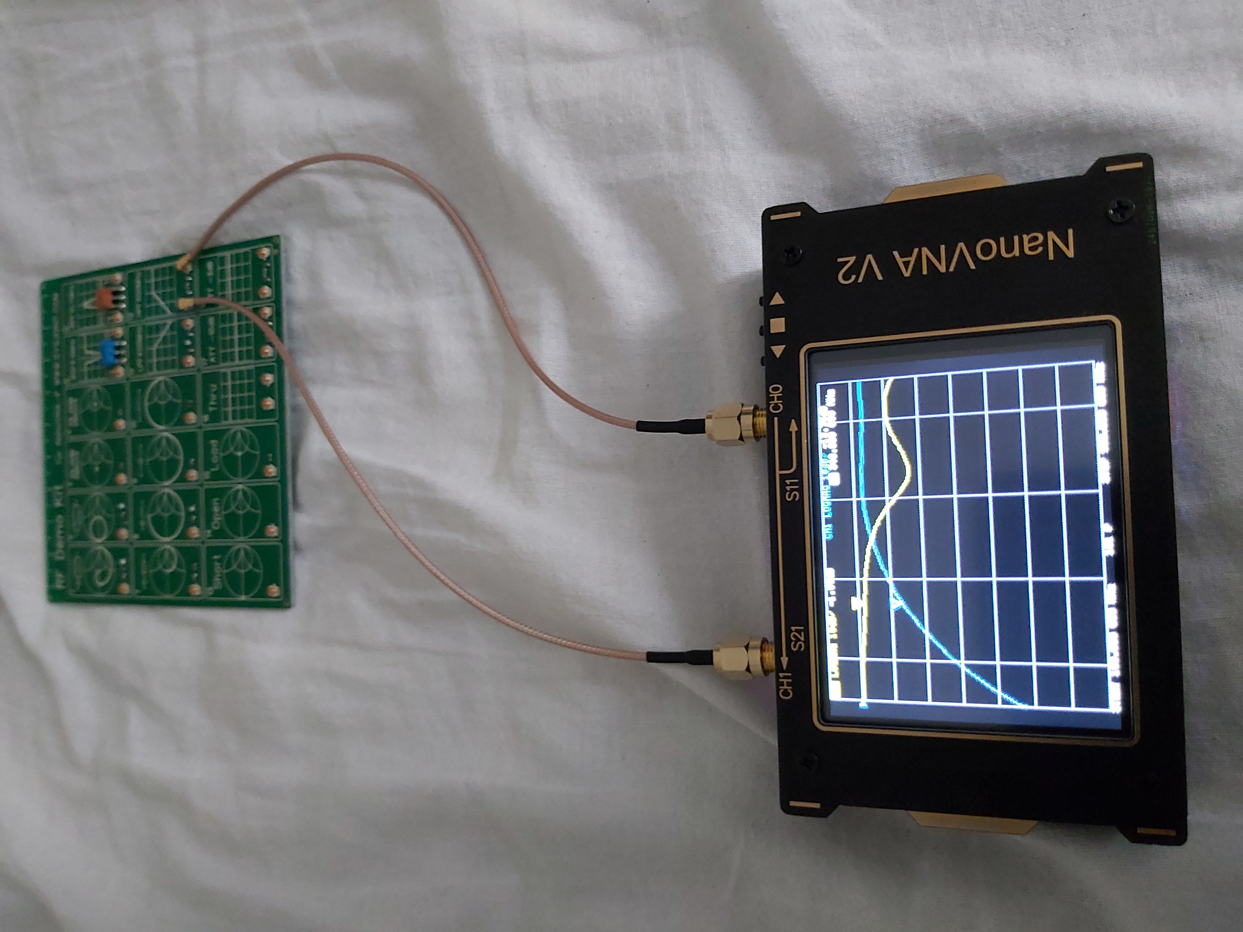
Got RF test kit to play with NanoVNA from Banggood: RF Demo Kit NanoVNA RF Tester Board Filter Attenuator for NanoVNA-F Vector Network Anaylzer. I selected this RF Demo Kit NanoVNA over another quite similar RF demo kit because this kit was cheaper and looked better.
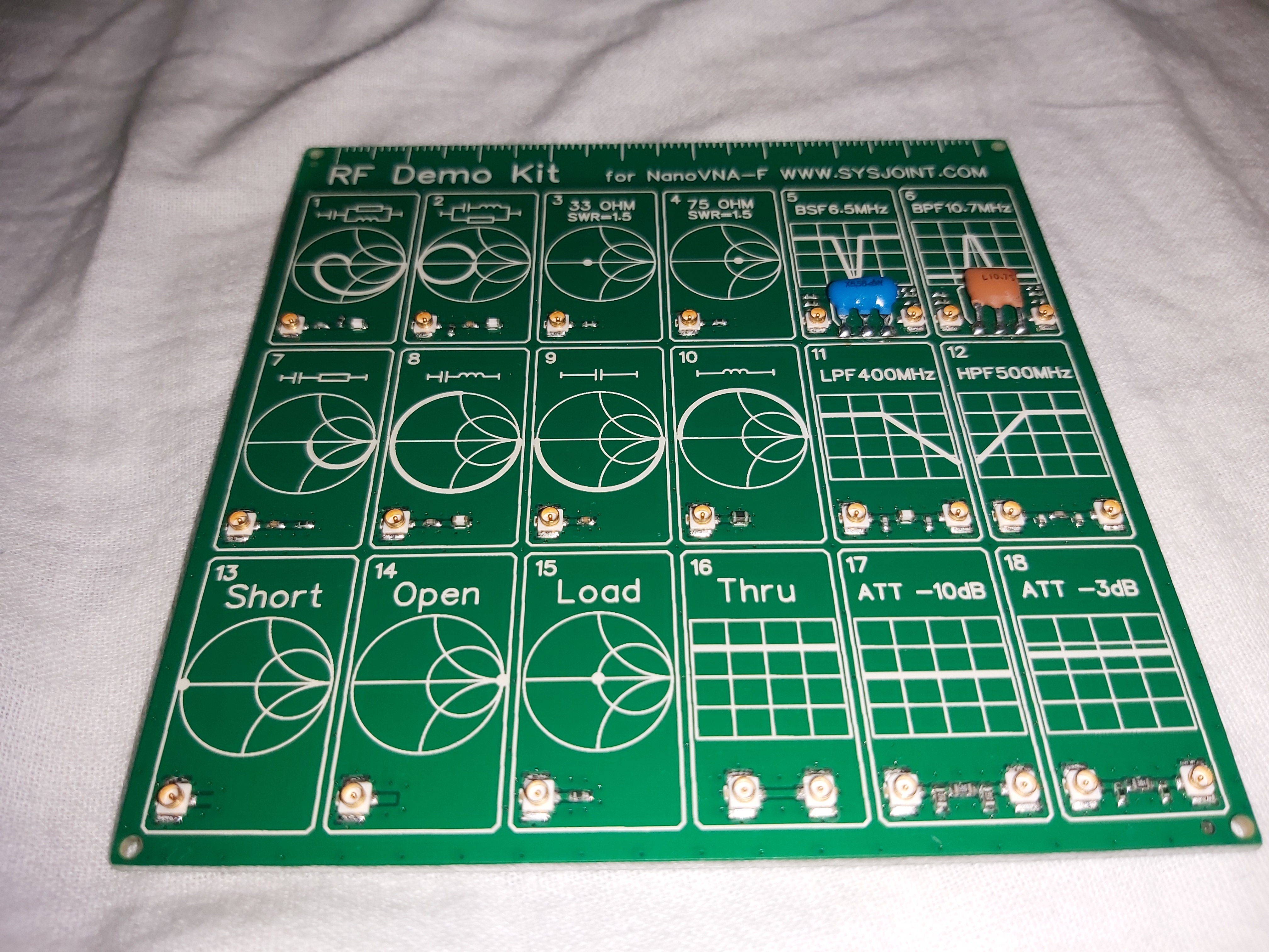
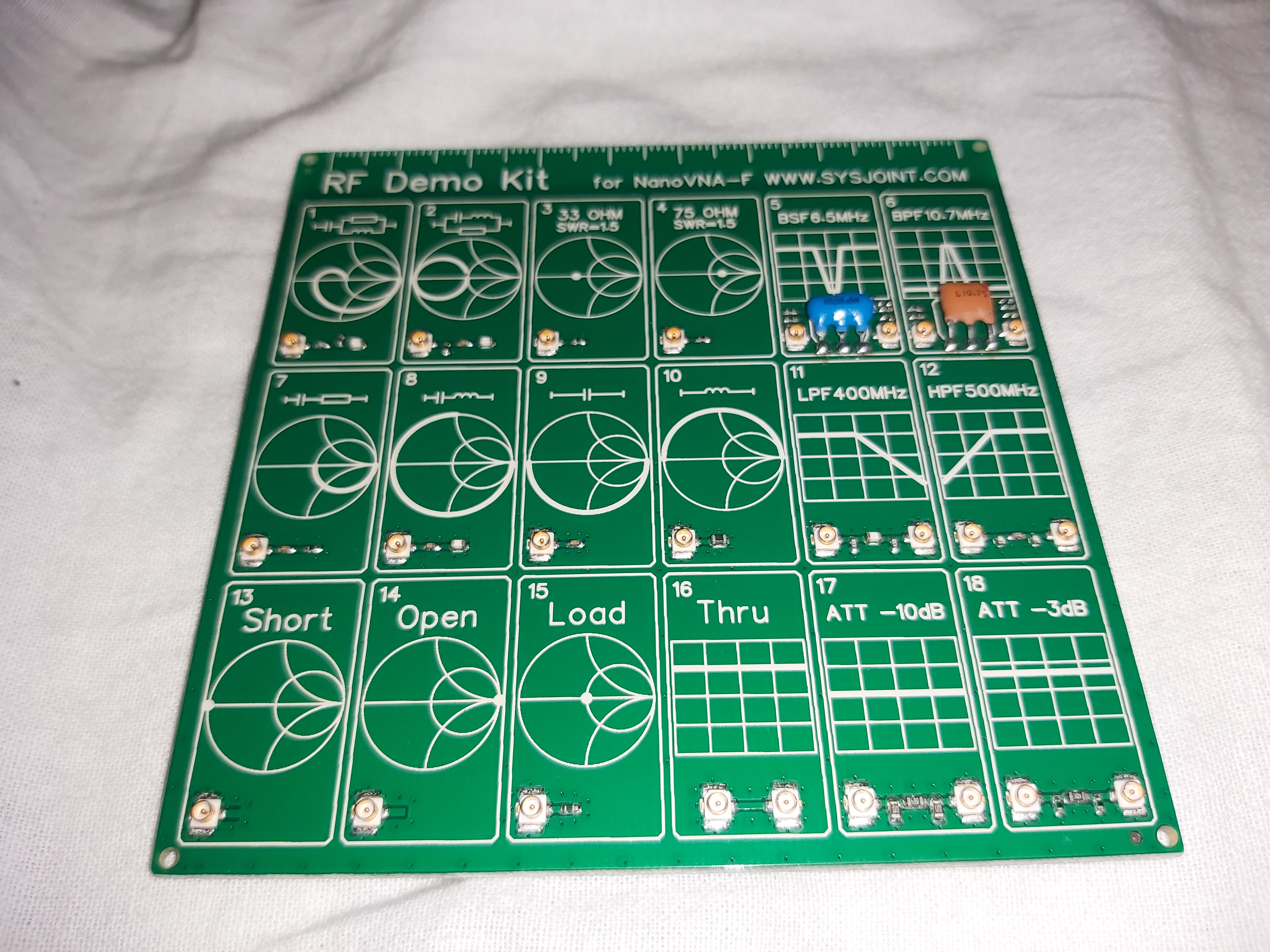
This RF Demo Kit is specially designed for RF Network Analyzer learners. It’s what I needed to learn how to use NanoVNA well and learn more about RF circuits. This RF test kit contains totally eighteen types or RF circuits, among which eleven types are single-port networks, and seven are dual-port networks. All the RF circuits on the board are terminated to UFL connectors (depending on the circuit one or two UFL connectors). The board came with two UFL – SMA test cables to connect the board to NanoVNA.
The board is equipped with three well-performing (open-short-load) calibrators which the operator can use to perform calibration with on the VNA before measuring. Calibration is a very good idea to get accurate measurement results.
RF Demo Kit NanoVNA RF Tester Board Filter Attenuator for NanoVNA-F Vector Network Anaylyzer product page has following description:
- PCB board in size of 10 x 10cm
- Vector network analyzer learner tool
- RLC series and parallel circuit 1
- RLC series and parallel circuit 2
- 33 ohm resistance, SWR=1.5
- 75 ohm resistance, SWR=1.5
- BSF ceramic notch filter, center frequency 6.5MHz
- BPF ceramic filter, centre frequency 10.7MHz
- RC series circuit
- LC series circuit
- Capacitor
- Inductance
- Homemade low-pass filter, 3dB bandwidth 400MHz
- Homemade high-pass filter, 3dB bandwidth 500MHz
- Short-circuit calibration circuit
- Open-circuit calibration circuit
- 50 ohm load calibration circuit
- Straight-through
- 10dB attenuation circuit
- 3dB attenuation circuit
Applications:
- Can be used with NanoVNA-F to measure 6.5M ceramic notch filter
- Can be used with NanoVNA-F to measure homemade low-pass-filter, 3dB bandwidth about 400MHz
Package Includes:
1 x PCB RF Tester Board
2 x 20cm Adapter Cables
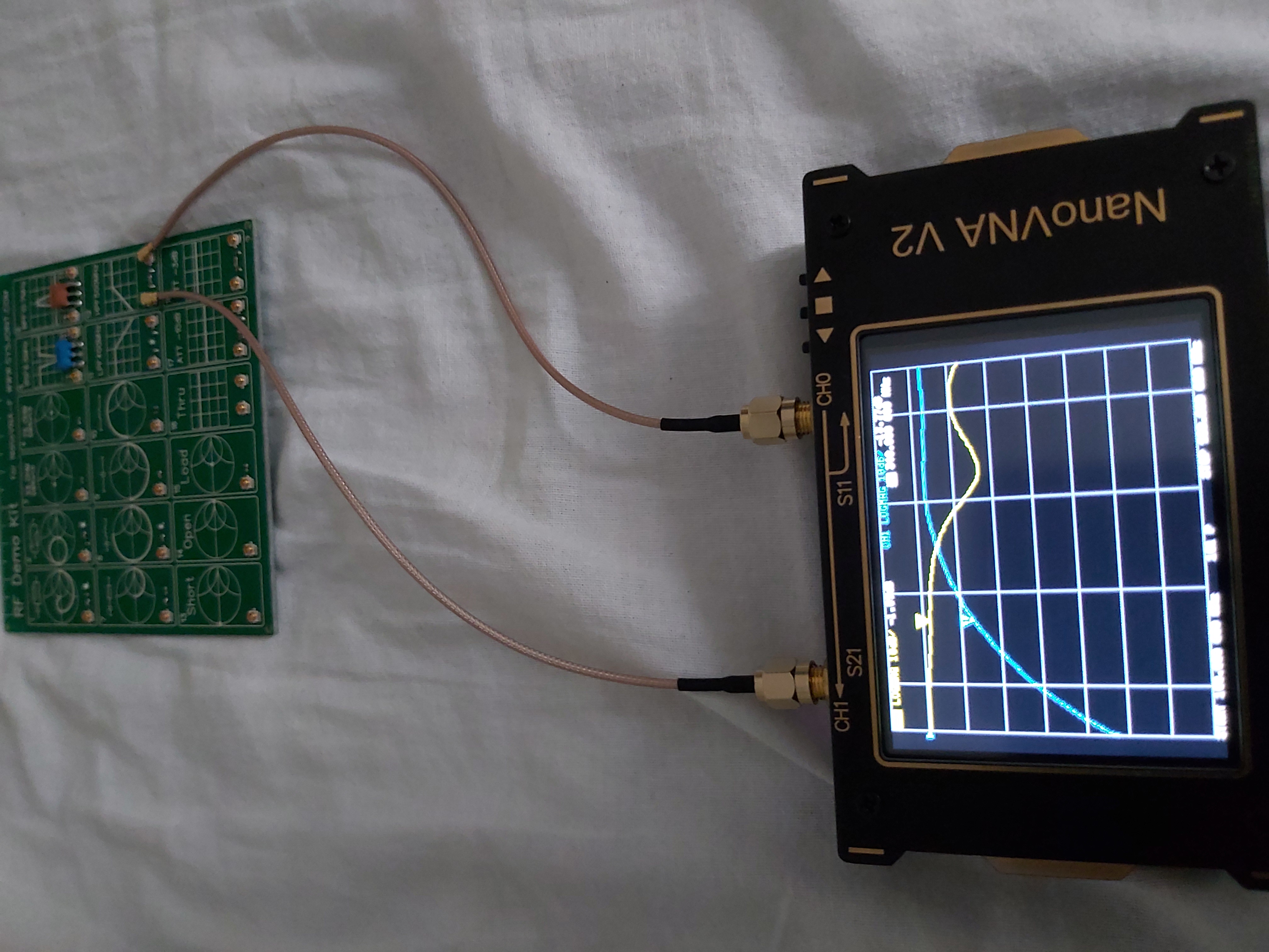
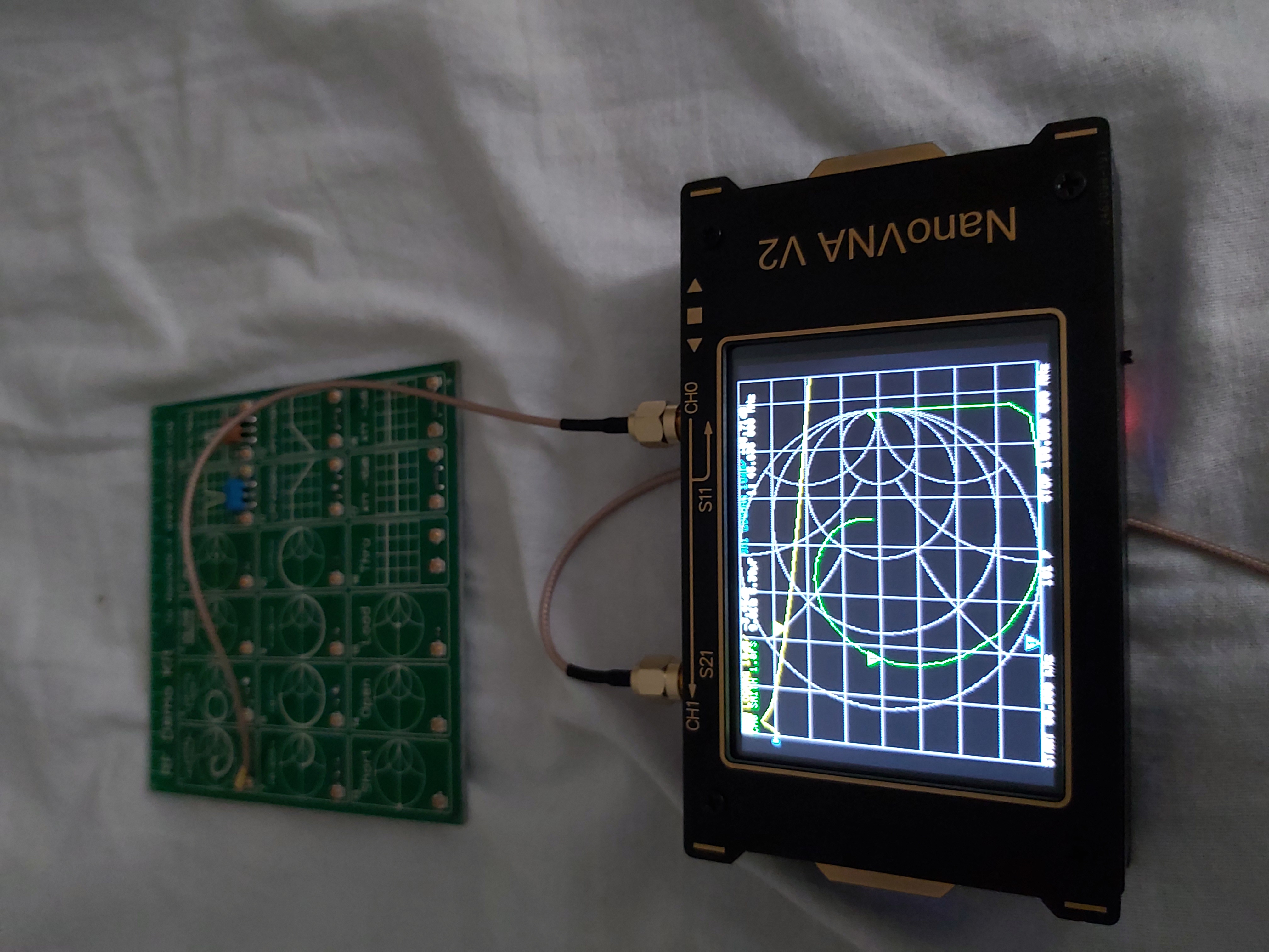
The board says that it is designed for NanoVNA-F, but I figured that there should not be any problem in using some other NanoVNA model. When I ordered this kit, I got the original NanoVNA. But later I received NanoVNA v2 that I did most testing with this board. The measurement results on this page are made with NanoVNA v2.
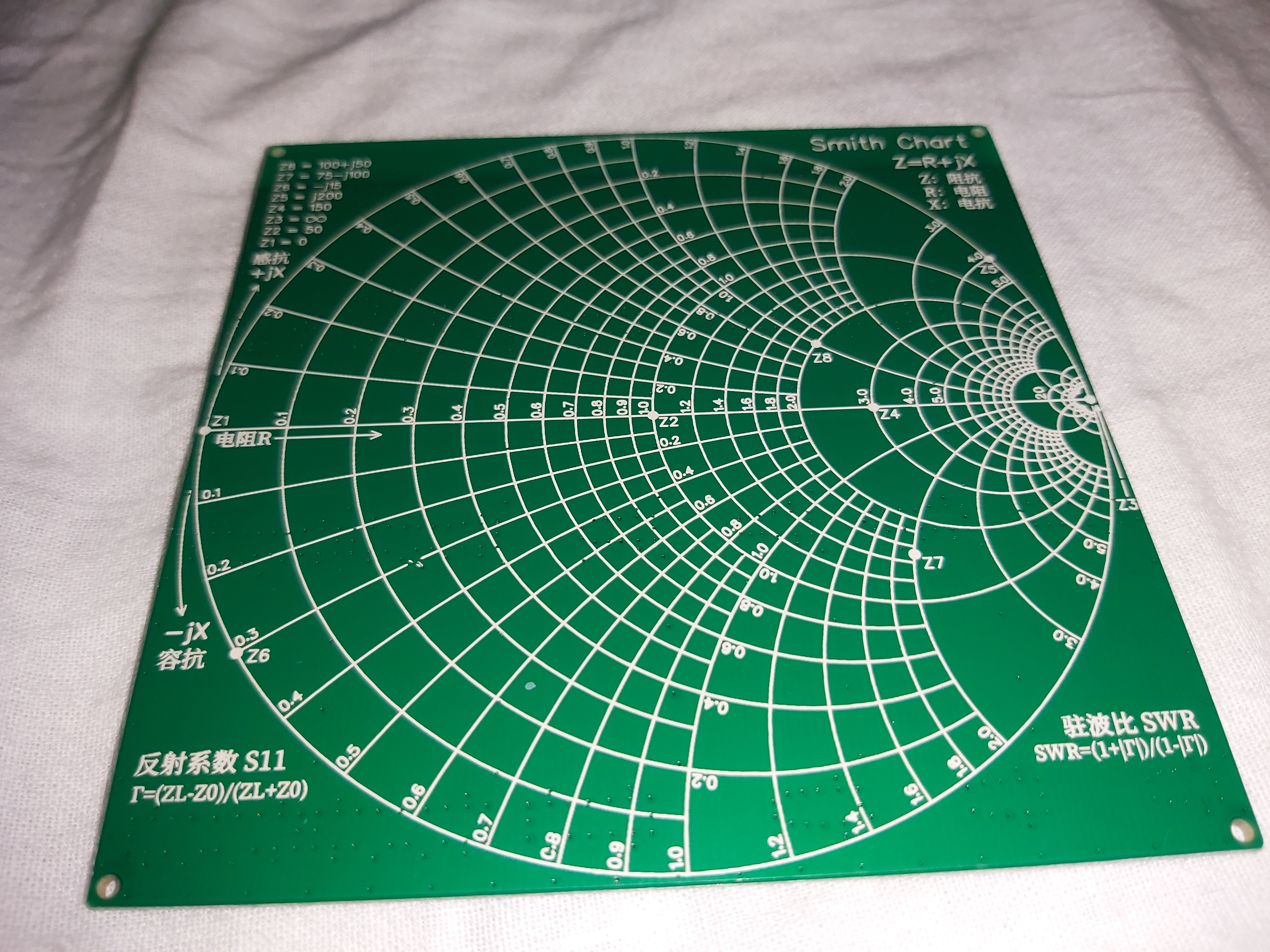
There is a Smith chart diagram on the backside of the circuit board:

This tester board came well packed with all the necessary leads to connect it to the board. This is excellent for educational purposes. It looks like a good board for learning about the use of the NovaVNA test unit. The build quality seems to be very with clear screen printing on the PCB to help with use. It looks to be worth the wait and the money. It is excellent for demonstrating and checking NanoVNA.
For low and high pass full default to 900 MHz scan range for NanoVNA is OK and gives good results.
With many circuits that showed different Smith chart images on the board, it seemed that the drawing on the board did not always match anywhere closely to the drawing. It took some time to figure out, that to get shapes on most circuit drawings to match what I see on NanoVNA screen, it is a good idea to check scan range from 50 kHz to 150 MHz. If I go higher than this stop frequency I get all kinds of strange shapes after when I want to get. If I go lower max frequency I don’t get full shape on the screen.
I am not the one that has found this limitation, from kit discussion:
In Test field 8 the inductor looks like to have nominal 470 nH.
If you accept a tolerance of +/- 10 % = 423 – 517 nH,
the usable frequency range is measured to 3.4 – 126 MHz.
Above 394 MHz the inductor becomes capacitive.
To get best results the tutorial posted to nanovna discussion group has some useful notes on testing:
Please note this, two steps must be performed before testing:
Step 1. Connect the two 20CM SMA to IPEX adapter cables to the NanoVNA-F machine.
Step 2. Recalibrate the machine using the 13 Short, 14 Open, 15 Load, and 16 Thru circuits on the test board, and save the parameters in 0.
There is a full tutorial at http://deepelec.com/rf-demo-kit/ and wiki page at https://groups.io/g/nanovna-users/wiki/RF-Demo-Kit-use.
This test kit is a very good idea. But there are some things that could maybe be improved. The UFL connectors on the board are very small. Little bit hard to see and use. And they feel fragile that they might not last very long. The micro coax plug is named U.FL/IPX, 50 Ohm, about 2mm diameter. For more details see on https://en.wikipedia.org/wiki/Hirose_U.FL. On the RF characteristics those connectors seem to be good, but the on the mechanical side they do not seem to be a good choice for this kind of test kit. Excerpt from Wikipedia page: “Female U.FL connectors are not designed with reconnection in mind, and they are only rated for a few reconnects (approximately 30 mating cycles [5]) before replacement is needed. The female U.FL connectors are generally not sold separately, but rather as part of a pigtail with a high-quality 1.32 mm doubly shielded cable, which allows for a low-loss connection.” It seems that the problem is the connector used on that is totally unsuitable. It is not
designed for repeated connections. Even the original manufacturer of the device, Hirosose, rate it at 20 connections/disconnections or *Durability* the number *30*. This means that the number of plugging cycles for an U.FL plug is a *minimum of 30*, with a *good probability of more*, if you handle it *careful*.
Please note that according to manufacturer you should use a special tool for removing them. This tool is made by Hirose, who designed the U.FL connector. Unfortunately it is *more expensive* than the *RF Demo Kit*. You can use a 1.0 mm wide flat screw driver for extracting. Up to now it works fine, if you press the cable down with your finger,
while you are levering with the screwdriver.
Every cheap similar looking connector is going to be some variation on that, and I suspect that they do not have longer designed service life than the original connector. I think you can expect problems sooner or later. If you handle the U.FL connector *careless*, you will have sooner or later a *problem*. If you plug and unplug it many times, you can expect to get problems. There are 25 connectors on the board, on 18 Test fields. So, if you test and document each Test field once, including calibration, you are still under the number of 30 cycles. I personally don’t think they will last long in the hands of a ham trying to learn, or demonstrate it to others.
21 Comments
Tomi Engdahl says:
#574 NANOVNA RF Demo Board SMA Version
https://www.youtube.com/watch?v=2W0pjMk56rA
NANOVNA-Demo-Board-SMA
https://github.com/imsaiguy/NANOVNA-Demo-Board-SMA
This is a version of the RF Demo Board. This one uses SMA connectors The RF Demo board uses a 0.032″ board.
Tomi Engdahl says:
#517 NANOVNA RF Demo Board
https://www.youtube.com/watch?v=SneOI7l5Kw4
Just as a note: when changing the span/center frequency, the VNA should be recalibrated.
run 3 says:
I tried to learn it, you share it great, thanks for the article. run 3
Tomi Engdahl says:
#574 NANOVNA RF Demo Board SMA Version
https://www.youtube.com/watch?v=2W0pjMk56rA
NANOVNA-Demo-Board-SMA
https://github.com/imsaiguy/NANOVNA-Demo-Board-SMA
Tomi Engdahl says:
Another kind of demo/test board designed for building your own RF filters
NanoVNA Testboard Kit VNA Vector Network Analysis Test Demo Board GQ
https://www.aliexpress.com/i/4001190520713.html?spm=2114.12057483.0.0.6f2326aciTraDN
https://www.aliexpress.com/item/4001190520713.html?spm=2114.12057483.0.0.6533666fT01HbA
Tomi Engdahl says:
Another type RF demo kits
download this presentation : http://www.sdr-kits.net/DG8SAQ/VNWA/VNWA_Experiments.pdf
Lots of examples in there on how to use and test with the NanoVNA (compatible with your board).
Edit : also checkout https://www.sdr-kits.net/DG8SAQ-VNWA-Testboard-kit (instruction manual, layout / trace labels etc).
Tomi Engdahl says:
And when you want inspirations, check out : https://www.ph2lb.nl/blog/index.php?page=qrp-labs-filter-adapter-for-nanovna#pcb20200527
Tomi Engdahl says:
#365a NANOVNA resistance measurements new calibration
https://www.youtube.com/watch?v=Xq86EMniXhM
Tomi Engdahl says:
https://www.rudiswiki.de/wiki9/nanoVNA
Tomi Engdahl says:
nanoVNA – Measuring Inductors and Capacitors Version 2 – VE6WGM
https://m.youtube.com/watch?v=CkJ0LjK-UGA&feature=youtu.be
Tomi Engdahl says:
nanoVNA – Measuring Inductors and Capacitors (Vers. 3)
https://m.youtube.com/watch?v=iJ1qKE5O0bY&feature=youtu.be
Tomi Engdahl says:
Understanding the Smith Chart
https://www.youtube.com/watch?v=rUDMo7hwihs
The Smith chart is one of the most important tools in understanding RF impedance and matching networks. This brief tutorial explains what the Smith chart is and how it can be used to represent complex impedances.
Download our free VNA Fundamentals Primer:
https://www.rohde-schwarz.com/us/products/test-and-measurement/network-analyzers/fundamentals-of-vector-network-analysis_253352.html?cid=802_us_smo_ALL__20-09_a______yt_TMfundmntls_Smith-Chart
Tomi Engdahl says:
https://www.edn.com/the-math-behind-the-smith-chart/
Tomi Engdahl says:
TRL Calibration
https://www.mariohellmich.de/projects/trl-cal/trl-cal.html
Besides the well known SOLT calibration method (or TOSM in Rohde & Schwarz terms) there are a number of other ways to achieve a full two-port calibration of a vector network analyzer (VNA). One of them is the thru-reflect-line calibration (TRL). As its name implies, TRL uses a through standard, a reflect standard, and one or more transmission lines of appropriate length for the intended frequency range to determine the error terms of the underlying error model, which is somewhat different than the model commonly used for TOSM (but can be mapped to the traditional and more comprehensive error model if some additional quantities, the switch terms, are known).
In TOSM, the match standard is instrumental for calibrating to system impedance. This role is played by the impedance of the line(s) in TRL.
TRL has the drawback that since the phase shift of the line standard must be within certain limits, it only works over a limited frequency band, and it cannot be sensibly used with very low frequencies (but can be extended to low frequencies by other means).
The TRL board
The most simple way to manufacture a test fixture for components like SMD capacitors, inductors, ferrite beads, etc., is to realize it on an ordinary PCB that can be produced with one of the many inexpensive PCB pool services. This allows putting the necessary TRL calibration standards on the board as well. Certainly this does not yield the most accurate test fixture, in particular if the board is ordinary FR4 and one saves on an impedance controlled service, but it has the advantage that the components are tested in their natural environment.
The TRL board that I have designed can be seen in the above picture. It contains the following features for calibration, verification, and testing:
A thru standard for TRL
A 50 Ohms match standard
A 25 Ohms mismatch standard for verification
An open standard for verification
A short standard, used as a reflect standard for TRL
A line of 45 mm length, used as a line standard for TRL
A series fixture for 0805 components
A shunt fixture for 0805 components
The board is designed to be usable up to about 2 GHz (it fails to achieve that, see below).
Tomi Engdahl says:
nanoVNA – measure Transmission Loss – example 1
https://owenduffy.net/blog/?p=19795
Tomi Engdahl says:
https://www.rudiswiki.de/wiki9/nanoVNA-Applications#nanoVNA_Applications
Tomi Engdahl says:
https://www.nonstopsystems.com/radio/frank_radio_coax-sw.htm
NOTE: the measurement techniques discussed below are not exclusively specific to the miniVNA. They are equally applicable to, e.g, the increasingly popular nanoVNA. The CH0 port of the nanoVNA corresponds to the Device Under Test (DUT) port of the miniVNA, and CH1 to the Detector (DET) port of the miniVNA.
Tomi Engdahl says:
https://www.edn.com/a-smith-chart-for-component-characterization/?utm_content=buffer1386c&utm_medium=social&utm_source=edn_facebook&utm_campaign=buffer
Tomi Engdahl says:
NANOVNA-Demo-Board-SMA
Gerbers for board
https://github.com/imsaiguy/NANOVNA-Demo-Board-SMA
This is a version of the RF Demo Board. This one uses SMA connectors The RF Demo board uses a 0.032″ board.
Tomi Engdahl says:
https://www.facebook.com/groups/368777730463838/permalink/776950559646551/
The “RF Demo Kit” for testing NanoVNA has no information about the component values, which make it less useful for testing and practical demonstration of a VNA. I used my Der EE DE-5000 LCR-meter to find the values, as this instrument can measure L, R and C even when mounted in a complex circuit. Also this instrument use Kelvin-measurements, with 4wires to the probe tips. Inductance, capacitance and resistance in the test leads will therefore not have any influence on the test results. My “Demo Kit” is the type with a 6.5MHz BSF and 433MHz BPF. There is another version too on the market, with 10.7MHz BPF, and probably other values for the components. The results are below:
LPF30: 195pF/0.8uH/195pF, HPF100: 170nH/C/170nH (not able to get the value for C here, but I wouldn’t be surprised if it is 100pF), 7: 100pF, 8: 760nH, 9: 100pF/50 ohm, 10: 225nH/100pF, 11: 100pF/220nH/50 ohm, and 12: 50 ohm/220nH/100pF.
Tomi Engdahl says:
#278: Smith Charts: Use SimSmith to design L Matching Networks
https://www.youtube.com/watch?v=f8MhMl4IqUE
https://www.w0qe.com/SimSmith.html