Nowadays you can find many low-cost microcontroller devboards (starting from just few dollars/euros). More recently, we’ve seen ARM Cortex kits for $10-$50, the flowering of the whole Arduino ecosystem, and of course, the Raspberry Pi. It’s microcontroller heaven with very many dev boards available. You you want more performance, there is a wide selection of Linux friendly single board computers in around $35 to $200 range.
What do you want to try next after microcontroller dev boards? Maybe FPGA. A field-programmable gate array (FPGA) is an integrated circuit designed to be configured by a customer or a designer after manufacturing. FPGAs contain programmable logic components called “logic blocks”, and a hierarchy of reconfigurable interconnects that allow the blocks to be “wired together” – somewhat like many (changeable) logic gates that can be inter-wired in (many) different configurations. Logic blocks can be configured to perform complex combinational functions, or merely simple logic gates like AND and XOR.
Those of us wanting a cheap “in” to the FPGA world have been less lucky than developers looking for microcontroller dev boards. FPGA boards under $100: Introduction article is indicting that the times, they are a changin’. Many FPGA devkits, from both chipmakers and third parties, have broken – or downright shattered – the $100 barrier, opening the door to low-cost FPGA prototyping, education, hobby projects, and so on. FPGA boards under $100: Introduction article offers a good overview of what is available.
Here are some interesting additions to the listed boards:
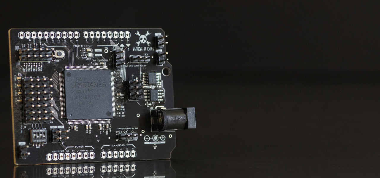
Hacklet 28 – Programmable Logic Hacks posting tells about Arduino-Compatible FPGA Shield. The shield features a Xilinx Spartan 6 FPGA and is available in The Hackaday Store. It has the needed regulators and level shifters. The price is $69.97. Not sure where to start? Check out Spartan-6 FPGA Hello World! that uses Xilinx’s free tool chain to getting a “hello world” led blinker running!
Hacklet 28 – Programmable Logic Hacks posting also mentions Chameleon. Chameleon is an Arduino compatible FPGA board with a Xilinx Spartan 3A FPGA on-board. The Chameleon Arduino-compatible shield board was designed to support two general application areas: (1) soft-core processors, and (2) intelligent serial communications interface.
Cheap FPGA-based HDMI Experimenting Board project is designing a (relatively) cheap little board for experimenting with HDMI using a Spartan-6 FPGA.
431 Comments
Tomi Engdahl says:
XuLA2-LX9 FPGA Board
http://store.hackaday.com/products/xula2-lx9
The XuLA2-LX9 FPGA Prototyping Board packs a 600-Kgate FPGA, 32 MB SDRAM and MicroSD card socket into two square inches of real estate.
$69.97
Just plug the XuLA2 into your circuit and connect a USB cable to download and test your design. Once you have your design just the way you want it, you can program it into the Flash and the XuLA2 will load it whenever power is applied. It’s really that simple.
Tomi Engdahl says:
Introducing the Cubic Board — A Completely Open Source FPGA Project
http://www.eetimes.com/author.asp?section_id=36&doc_id=1326702&
One of the main design considerations for the FPGA-based Cubic Board was to make it easily accessible to both software and hardware developers.
One idea I proposed was a “pocket-change” FPGA board with a sticker price of $9.99. That particular idea never went any further, although one unassuming guy in the group later pulled me to one side to describe how he was building an FPGA board based on a very similar concept. This person turned out to be Bo Zhou.
The original revision of Bo’s board used a Cyclone IV E FPGA and was named “Cubic Board” (Compact Cyclone Core, C3). The motivation was to build an FPGA module that would be usable across many types of project. This was based on the observation that traditional FPGA development boards were built for educational or lab-evaluation purposes, and so would not necessarily be optimized for production use. Also, there were only a few FPGA modules on the market similar to the Cubic board concept; all of them seemed rather expensive; and none of them were open sourced.
Thus, Bo decided to design and build his own cost-optimized, yet industrial-strength FPGA module.
This concept soon became popular among Altera makers. One of the other team members for this project, Chris Rauer, used his embedded software expertise to quickly port Linux onto the board utilizing Altera’s soft-core NIOS processor and created a python library to control the GPIO.
This feedback resulted in Rev 2 of the board, which instantiated the Cyclone V SoC FPGA device and was imaginatively dubbed the Cubic SoC Board. This Altera FPGA is a 28nm device (compared to the 45nm Cyclone IV device) and contains dual ARM Cortex-A9 hard processor cores as well as a hardened DDR memory controller and multi-gigabit transceiver channels. The form factor of the board was also changed to a 70mm by 33mm rectangular size with a single edge connector
Rev 2 Cubic Board having a full software stack, including embedded Linux support, various drivers, and multiple demo programs.
One of the other main design considerations for this board was to make it easily accessible to both software and hardware developers.
First, the Cubic board is positioned to be an open-source project and we believe this is the first ever open source FPGA board ever made.
Second, having “hard-to-design” hardware features integrated into the Cubic SoC’s compact SoM form-factor — for example, designed and proven LPDDR2 memory and USB interfaces — enables the developer to focus on more value added design work.
Third, the SoM has a Linux image ready to boot, so the software developer could quite easily get I/O pins toggling within minutes.
Altera provides free versions of all the tools necessary to program the hardware and software for the Cyclone V SoC FPGA — namely, Quartus II for programming the FPGA fabric, and EDS for software development (click here for more details). Now, while this suite of tools is really nice, it is still pretty complex to use, and it takes a lot of effort to get a system like this up and running, so we developed a virtual machine to largely remove this complexity for the user.
We believe the Cubic SoC board has a lot more performance and capability than other similar products out there (e.g., Arduino or Raspberry Pi) and — using the Cyclone FPGA’s pin migration capability — adding additional hardware resources by building the same board with a larger capacity FPGA is possible.
All that processing power does, however, come at a price premium, probably retailing for sub-$200, which we believe is still very accessible for many hobbyists and commercial product developers.
Tomi Engdahl says:
Two New Dev Boards That Won’t Make Your Wallet Hurt-So-Good
http://hackaday.com/2015/06/13/two-new-dev-boards-that-wont-make-your-wallet-hurt-so-good/
DE0 Nano SoC
First, the dev board boasts a Cyclone V with 40,000 logical elements (up from the DE0’s 22K) and an integrated dual-core Arm Cortex A9 Processor. The PCB layout also brings us 3.3V Arduino shield compatibility via female headers, 1 Gig of external DDR3 SDRAM and gigabit ethernet support via two onboard ASICs to handle the protocol. The folks at Terasic also seem to be tipping their hats towards the “Duino-Pi” hobbyist community, given that they’ve kindly provided both Linux and Arduino images to get you started a few steps above your classic finite-state machines and everyday combinational logic.
The board hits online shelves now at a respectable $100.
DE0-Nano-SoC Kit/Atlas-SoC Kit
http://www.terasic.com.tw/cgi-bin/page/archive.pl?Language=English&No=941
Tomi Engdahl says:
the Chinese are doing some interesting entry level FPGA boards. For about £40 you can get a board with a Cyclone IV, 32MB of SDRAM, 16 bit VGA port, PS/2 port, SD card reader, RTC, JTAG programmer etc. You don’t get a huge amount of capacity for that price, but plenty enough for 8 bit system emulation
Source: Comment at http://hackaday.com/2015/06/13/two-new-dev-boards-that-wont-make-your-wallet-hurt-so-good/
Tomi Engdahl says:
Hackaday Prize Entry: They Make FPGAs That Small?
http://hackaday.com/2015/07/03/hackaday-prize-entry-they-make-fpgas-that-small/
. Meet DIPSY, the FPGA that fits in the same space as an 8-pin DIP.
FPGAs are usually stuffed into huge packages – an FPGA with 100 or more pins is very common. [antti] found the world’s smallest FPGA. It’s just 1.4 x 1.4mm on a wafer-scale 16-pin BGA package. The biggest problem [antti] is going to have with this project is finding a board and assembly house that will be able to help him.
The iCE40 UltraLite isn’t a complex FPGA; there are just 1280 logic cells and 7kByte of RAM in this tiny square of programmable logic. That’s still enough for a lot of interesting stuff, and putting this into a convenient package is very interesting. The BOM for this project comes out under $5, making it ideal for experiments in programmable logic and education.
open source toolchain for iCE40 FPGAs
DIPSY
FPGA Module priced at 5 USD
https://hackaday.io/project/6592-dipsy
Tomi Engdahl says:
Zynq and the OPL3 Music Synthesizer
http://hackaday.com/2015/08/10/zynq-and-the-opl3-music-synthesizer/
We’re big fans of the Zynq, which is an answer to the question: what do you get when you cross a big ARM processor with a big FPGA? So it isn’t surprising that [GregTaylor’s] project to emulate the OPL3 FM Synthesis chip in an FPGA using the Zynq caught our eye.
The OPL3 (also known as the Yamaha YMF262) was a very common MIDI chip on older PC sound cards. If you had a Sound Blaster Pro or 16 board, you had an OPL3 chip in your PC. The OPL3 was responsible for a lot of the music you associate with vintage video games like Doom.
Reverse engineered SystemVerilog RTL version of the Yamaha OPL3 (YMF262) FM Synthesizer
https://github.com/gtaylormb/opl3_fpga
Reverse engineered SystemVerilog RTL version of the Yamaha OPL3 (YMF262) FM Synthesizer. Design is complete and working on the Digilent ZYBO board. Further testing is needed to verify full functionality and coverage. I’ll mostly be adding and working on the software at this point.
Tomi Engdahl says:
ICEd = an Arduino Style Board, with ICE FPGA
ICEd = Arduino Compatible Board supported by free vendor Tools and by open-source FPGA tools.
https://hackaday.io/project/6636-iced-an-arduino-style-board-with-ice-fpga
Directly supported by Lattice Development tools
Supported by open-source FPGA tools, project “icestorm”
FPGA pinout mostly compatible to Lattice iceStick development board
1 Digilent Pmod(tm) slot
FT2232H, use for Flash Programming or FPGA download to RAM
Tomi Engdahl says:
DIPSY
DIY System on Chip based on FPGA, priced below 5 USD
https://hackaday.io/project/6592-dipsy
DIY Yourself System On Chip, at below 5 USD pricing, hacking friendly, small and low power.
Sized 10x10mm, priced sub 5 USD (BOM price approx 1.5 USD) FPGA Module with ultra low power consumption. Easy accessible 100mil pin header style design.
Can be used “custom IC” when the FPGA OTP internal NV memory is burned or as coprocessor or accelerator for slow microcontrollers configured over SPI interface.
5 grains of Sand (as per classification Sand grain is a particle smaller than 2mm):
iceUL1K-SW16 has metric size of 1.4×1.4×0,45 mm
TLP713 small and tiny LDO needed to power the brains, sized 1x1x0.45 mm
Capacitor 0201 size
Capacitor 0201 size
Resistor 0201 size
This is all you need to build a custom System on Chip, all you need are 5 grains of Sand.
Tomi Engdahl says:
Nyx: Edison – FPGA Devboard
https://hackaday.io/project/7500-nyx-edison-fpga-devboard
A development board with:
Spartan 6 LX25
Intel Edison
Arduino Compatible headers (3.3V)
8 x PMOD connectors
4 x SATA connectors (used for 8 differential signal connections)
Select-able voltage for the differential and lower 4 PMODs 1.2V, 1.8V, 2.5V and 3.3V
Dionysus is a Spartan 6 LX9 Development board with 8MB of 100MHz SDRAM and a fast USB – FIFO interface between the host computer and the FPGA. It has served me well, I’ve developed a camera and LCD demo (Video below) as well as exercised most of the Nysa tool
Tomi Engdahl says:
‘FleaFPGA Uno’ Experimenter’s board
https://hackaday.io/project/7043-fleafpga-uno-experimenters-board
attempt at making a powerful and Flexible (and somewhat Arduino®-compatible) solution based on the Lattice MachXO2 FPGA
Basically, FleaFPGA Uno is an Arduino®-compatible board with the following features:
- Lattice MachXO2-7000 FPGA with on-board JTAG and serial via microUSB
- Digital Video out.
- Configurable PS2 or USB host interface.
- 512KByte fast SRAM
- 16MByte user SPI Flash ROM
- Composite analog video and stereo audio (AV) out.
- Six high-speed ADC and also 16 x Digital GPIO.
- (optional) WIFI interface.
Tomi Engdahl says:
SmartFusion2 development kit comes with JTAG emulator
http://www.edn.com/electronics-products/other/4440431/SmartFusion2-development-kit-comes-with-JTAG-emulator?_mc=NL_EDN_EDT_EDN_today_20150928&cid=NL_EDN_EDT_EDN_today_20150928&elq=c1005f1dfbc94102961e3ab2814e2e6c&elqCampaignId=24949&elqaid=28312&elqat=1&elqTrackId=2e22587cfa9b4dc0be03fbc77c0e1e81
Based on a SoC FPGA with embedded security, Avnet’s SmartFusion2 KickStart kit enables the prototyping of low-power, high-security IoT designs for the communications, medical, automotive, video, smart energy, and industrial markets. Unlike existing SmartFusion2 development boards, the Avnet KickStart board furnishes a JTAG emulator and power supply. The USB-powered board is also outfitted with a Microchip RN4020 Bluetooth Lower Energy module.
At the heart of the development board is the Microsemi M2S010S SmartFusion2, an SEU-immune SoC FPGA that integrates 10,000 logic elements and a 166-MHz ARM Cortex-M3 processor. The board’s Arduino-compatible interface and three 12-pin Pmod-compatible connectors allow the addition of existing custom modules to implement bridging, acceleration, or I/O expansion. Also included are onboard ambient light, motion, and temperature sensors; four user LEDs; and two user push-button switches.
Microsemi SmartFusion2 SoC FPGA KickStart Development Kit
http://www.em.avnet.com/en-us/design/drc/Pages/Microsemi-SmartFusion2-KickStart-Development-Kit.aspx?cmp=NA-AVT-PR-SF2KS-201509
Avnet’s SmartFusion2 KickStart Kit features the Microsemi M2S010S SmartFusion®2 SoC FPGA, a secure and integrated programmable system-on-a-chip device with 10k logic elements and a 166 MHz ARM® Cortex®-M3 processor. This low power SmartFusion2 device is flash-based and single event upset (SEU) immune
Low cost development kit, only $59.95!
Tomi Engdahl says:
ARMs and FPGAs Make for Interesting Dev Boards
http://hackaday.com/2015/10/07/arms-and-fpgas-make-for-interesting-dev-boards/
Tiny Linux computers are everywhere, and between BeagleBones, Raspberry and Banana Pis, and a hundred other boards out there, there are enough choices to go around. There is an extremely interesting ARM chip from Xilinx that hasn’t seen much uptake in the field of tiny credit-card sized computers: the Zynq. It’s an ARM Cortex-A9 coupled with an FPGA. It’s great for building peripherals that wouldn’t normally be included on a microcontroller. With Zynq, you just instantiate the custom bits in the FPGA, then interface them with a custom Linux driver. Thanks to CrowdSupply, there’s now a board out there that brings this intriguing chip to a proper development platform. It’s called the Snickerdoodle, and if you’ve ever wanted to see the capabilities of an FPGA tightly coupled to a fast processor, this is the board to watch.
The core of the Snickerdoodle is a Xilinx Zynq that features either a 667 MHz ARM Cortex A9 and a 430k gate FPGA (in the low-end configuration) or an 866 A9 and 1.3M gate FPGA. This gives the Snickerdoodle up to 179 I/O ports – far more than any other tiny Linux board out there.
https://www.crowdsupply.com/krtkl/snickerdoodle
snickerdoodle ($55)
A palm-sized Linux computer that connects to the real world with ARM, FPGA, Wi-Fi, Bluetooth, and 154 reconfigurable I/O. snickerdoodle is a brain for your robot, an autopilot for your drone, and the backbone for your computer vision system – all in one tight little package.
Tomi Engdahl says:
Evaluation kit jumpstarts FPGA embedded design
http://www.edn.com/electronics-products/other/4440528/Evaluation-kit-jumpstarts-FPGA-embedded-design?_mc=NL_EDN_EDT_EDN_today_20151008&cid=NL_EDN_EDT_EDN_today_20151008&elq=6a7bcb9354a7416d954435bd8197b9a7&elqCampaignId=25127&elqaid=28562&elqat=1&elqTrackId=35a6362c52d44966bcf707c4c6664879
Arty is a customizable evaluation kit from Avnet that allows developers to prototype low-power embedded designs based on the Xilinx Artix-7 35T FPGA. Along with the 33k-logic cell FPGA, the kit also features the Xilinx MicroBlaze soft processor core, which is customizable for virtually any processor use case.
The small form-factor Arty board supports multiple expansion options through an Arduino/ChipKit shield connector (49 I/O) and four Pmod interfaces (32 I/O).
Arty comes with a full Vivado Design Edition seat, enabling designers to develop embedded applications ranging from Linux-based systems to lightweight microcontroller projects. It also furnishes a reference design featuring MicroBlaze and FreeRTOS webserver.
The Arty evaluation kit costs $99.
http://www.em.avnet.com/en-us/design/drc/Pages/Artix-7-35T-FPGA-Evaluation-Kit.aspx?cmp=na-aes3-pr-201509
Tomi Engdahl says:
Open Source FPGA Pi Hat
http://hackaday.com/2015/10/10/open-source-fpga-pi-hat/
Over on Hackaday.io, [Dave Vandenbout] has posted the CAT board, a Raspberry Pi daughterboard hat that features a Lattice FPGA, 32 MB of RAM, EEPROM, and a few Grove and PMOD connectors. The CAT takes advantage of the open source tool chain available for Lattice including the Python-based MyHDL (although, you could just use Verilog directly, if you prefer) and Icestorm. One interesting point: you can run the tool chain on the Raspberry Pi, resulting in a self-contained and largely portable FPGA development environment.
The design files are actually on Github.
CAT Board
The CAT Board is part of a Raspberry Pi-based hand-held FPGA programming system.
https://hackaday.io/project/7982-cat-board
Tomi Engdahl says:
Simulating an analog computer on a FPGA
https://hackaday.io/project/259-simulating-an-analog-computer-on-a-fpga
Analog computers are completely parallel. FPGA simulation of integrators implements fast, parallel solution of differential equations.
Tomi Engdahl says:
Using FPGAs in embedded systems is getting easier
http://www.edn.com/electronics-blogs/now-hear-this/4440586/Using-FPGAs-in-embedded-systems-is-getting-easier?_mc=NL_EDN_EDT_EDN_today_20151014&cid=NL_EDN_EDT_EDN_today_20151014&elq=09e2706fd231453dbd0b6f9d6b6822b0&elqCampaignId=25216&elqaid=28688&elqat=1&elqTrackId=abd6048b5c6f44a9bbc7056ed02ae0b8
As Jason and Matt note in their session description:
Not all embedded designers have experience with FPGA design; for many, the leap to developing FPGAs can present a daunting obstacle. However, FPGA suppliers are giving rise to a new breed of SoC-based FPGAs that combine the power of advanced microprocessor cores with the programmable fabric of a standard FPGA. In addition, new FPGA development flows are opening the door for higher-level languages such as C or OpenCL to be mapped to the FPGA fabric.
Tomi Engdahl says:
FPGAs For The Raspberry Pi
http://hackaday.com/2015/10/18/fpgas-for-the-raspberry-pi/
FPGA development has advanced dramatically in the last year, and this is entirely due to an open-source toolchain for Lattice’s iCE40 FPGA. Last spring, the bitstream for this FPGA was reverse engineered and a toolchain made available for anything that can run Linux, including a Raspberry Pi. [Dave] from Xess thought it was high time for a Raspberry Pi FPGA board. With the help of this open-source toolchain, he can program this FPGA board right on the Raspberry Pi.
The inspiration for [Dave]’s board came from the XuLA and StickIt! boards that give the Raspberry Pi an FPGA hat. These boards had a problem; the Xilinx bitstreams had to be compiled on a ‘real’ PC and brought over to the Raspberry Pi world. The new project – the CAT Board – brings an entire FPGA dev kit over to the Raspberry Pi.
CAT Board
The CAT Board is part of a Raspberry Pi-based hand-held FPGA programming system.
https://hackaday.io/project/7982-cat-board
Tomi Engdahl says:
FPGA-based GPU
https://hackaday.io/project/8097-fpga-based-gpu
FPGA-based GPU with optimized SDRAM controller. Using the Terasic DE0-Nano and LT24 LCD. No NIOS!
Tomi Engdahl says:
Stuffing Macs Into FPGAs
http://hackaday.com/2015/10/24/stuffing-macs-into-fpgas/
A few years ago, [Steve] of Big Mess ‘O Wires fame stuffed one of the first Macintosh computers into an FPGA.
Now, there’s a new tiny FPGA board around, and this one is perfectly designed to fit the original Macintosh on it.
Plus Too Mac Replica, New Progress!
http://www.bigmessowires.com/2015/10/22/plus-too-mac-replica-new-progress/
Tomi Engdahl says:
‘Arduino on Steroids’: FPGA-based XLR8 at ESC Minneapolis
http://www.eetimes.com/author.asp?section_id=216&doc_id=1328060&
Even with the same clock frequency as a regular Arduino, the FPGA-based XLR8 can accelerate things like floating-point math and perform other tasks much better.
Alorium Technology will also be at ESC Minneapolis. And the reason that’s of interest is that these little scamps have created an FPGA-based board called the XL8R (“Accelerate” — get it?) that has the same footprint and behaves just like an Arduino Uno on steroids.
The regular Arduino Uno has a 16 MHz clock and does things in a certain way. The last thing a user wants to do is swap this out with something that runs much faster, for example, but that doesn’t work with any of that user’s existing shields. Thus, the XLR8′s FPGA has been configured to look exactly like the microcontroller (MCU) powering the Arduino Uno, down to the fact that it also employs a 16 MHz clock.
At this point you may be saying to yourself “But if it walks exactly like an Arduino Uno, and if it talks exactly like an Arduino Uno, then why don’t I just use an Arduino Uno and have done with it?” Ah, but there’s more… there’s so much more…
Let’s start with floating-point math, for example.
By comparison, the XLR8 has dedicated floating-point hardware programmed directly into the FPGA’s fabric.
And there’s more. One of the things a lot of Arduino users want to do is create robots and control servos. One of the problems is that servicing interrupts can result in “twitching” on the servos. By comparison, the XLR8 has dedicated servo functions
Well, I just got off the phone with Jason Pecor from Alorium Technology. Jason tells me that they are planning on tackling a variety of issues people have with the regular Arduino. And for each of these solutions, the user’s programs will remain unchanged apart from swapping out an existing library call with its XLR8 counterpart. For example, since so many people are using WS2812-based LEDs — like Adafruit’s NeoPixels — this is a target that’s firmly in Alorium’s sights, which explains why I’m currently performing my happy dance (avert your eyes; it’s not a sight for the young or faint-of-heart).
Accelerate Your Project with XLR8!
http://www.aloriumtech.com/
XLR8 Servo Control XB Demo
https://www.youtube.com/watch?v=EkSMqOB0pL4&feature=youtu.be
Tomi Engdahl says:
Programmable Logic: Build Yourself a CPLD Module
http://hackaday.com/2015/10/28/programmable-logic-build-yourself-a-cpld-module/
A Complex Programmable Logic Device (CPLD) is a great piece of hardware to have in your repertoire. As its name implies, you can program these chips to serve the logic functions you need. This might be replacing an obsolete chip, or maybe just a way to learn and try different techniques. What better way to learn than to get your hands on a CPLD and give it a try?
To implement an easily solderable kit I went with an older CPLD part that also has 3.3v and 5v versions that will maintain its programming regardless of power.
Looking at the schematic you can tell there isn’t much to it: basically the CPLD, the circuit for In Circuit Programming and an oscillator to drive the logic in the CPLD.
This part known as the EPM7032 and EPM7064, comes in a 44 pin Plastic Leaded Chip Carrier (PLCC)
The on-board oscillator is included so that the CPLD can do things statefully and create fast counters on its own without the need for an external clock.
Programming the CPLD
The 10 pin connector and a handful of resistors comprise the programming circuit.
To program a standalone CPLD like this, a dedicated programmer is needed. That’s easy for me to say as I usually have several lying around, but if you don’t have one it’s not too painful to get into the game. An approved “Altera USB Blaster” costs $50
Tomi Engdahl says:
Digilent ARTY is a $99 Xilinx Artix-7 FPGA Board with Arduino Headers
Read more: http://www.cnx-software.com/2015/10/02/digilent-arty-is-a-99-xilinx-artix-7-fpga-board-with-arduino-headers/#ixzz3q2OAGFQJ
Topic: Xilinx Arty US$99 FPGA board. Expert opinions please.
http://www.eevblog.com/forum/microcontrollers/xilinx-arty-us$99-fpga-board-expert-opinions-please/
Tomi Engdahl says:
FPGA-based GPU as high speed learning platform
https://hackaday.io/project/8097-fpga-based-gpu-as-high-speed-learning-platform
FPGA-based GPU with optimized SDRAM controller. Using the Terasic DE0-Nano and LT24 LCD. No NIOS!
I’m building a GPU to learn about FPGAs, high speed memories, bus access arbitration, PCI express, etc. Basically all the hard things that surround “okay it does some math.”
I find it easier to flesh out HaD project pages when the projects are finished. So for now, this project page serves as a sort of progress log.
Tomi Engdahl says:
Programmable Logic: Build Yourself a CPLD Module
http://hackaday.com/2015/10/28/programmable-logic-build-yourself-a-cpld-module/
A Complex Programmable Logic Device (CPLD) is a great piece of hardware to have in your repertoire. As its name implies, you can program these chips to serve the logic functions you need. This might be replacing an obsolete chip, or maybe just a way to learn and try different techniques. What better way to learn than to get your hands on a CPLD and give it a try?
I created a CPLD module with the intent of being able to plug it into lots of things including solderless breadboards
The CPLD: A surface mount part that fits a through-hole socket
Image-j-leadThis part known as the EPM7032 and EPM7064, comes in a 44 pin Plastic Leaded Chip Carrier (PLCC) or sometimes called J Lead due to the J shape of the pin leads. This package can be inserted in a through-hole socket or directly soldered to the PCB.
Tomi Engdahl says:
Make Electronics visually (arduino compatible)
Wikit: programmable hardware with flowchart
https://hackaday.io/project/8246-make-electronics-visually-arduino-compatible
Hardware is not hard with Wikit.
Wikit is an FPGA based platform co-work with iPAD.
It could enables your complex hardware development with flowchart methodlogy.
Feature:
1.Program with flowcharts. No programming skills required
2.Support transform Arduino code into Flowchart block
3.support over 100 modules on Sparkfun and Adafruit (keep growing)
How flowchart works
HW accessing:
Flowchart app on iPAD wikit
(Note: wikit could also return the data back to iPAD for algorithm)
wiki wifi module –direct interface–> send to FPGA module for actual physical access
Algorithm operation:
happens inside the Flowchart app on iPAD
More project details on http://wikit.co
Tomi Engdahl says:
Build an AM Radio Transmitter from a CPLD
http://hackaday.com/2015/11/12/build-an-am-radio-transmitter-from-a-cpld/
[Alex Lao] has been playing around with the CPLD-like parts of a PSoC. Which is to say, he’s been implementing simple logic functions “in hardware” in software. And after getting started with the chip by getting accustomed to the different clock sources, he built a simple AM radio that transmits at 24 MHz.
PSoC – AM Radio Transmitter
http://www.voltagedivide.com/2015/10/16/psoc-am-radio-transmitter/
NOTE: If you decide to recreate my experiment, you should take a look at your country’s regulations for radio communicating devices
Using the configurable logic in the PSoC, I have created a simple radio transmitter that transmits a string of random bits using a 24 MHz carrier wave.
With SDR# set to AM demodulation, a clear 1 KHz tone can be heard.
We can add more tones to transmit more bits per tone (or bits per symbol).
Pretty simple huh? With this setup, I was able to receive the tones one floor above where the dev-kit was sitting. Maybe in the future I will write a receiver program in GNU Radio or something similar, but for now, this is just a cool demo.
Tomi Engdahl says:
FPGA Interfaces Speeding Up
IBM/Xilinx collaborate, Red Hat wants standard
http://www.eetimes.com/author.asp?section_id=36&doc_id=1328278&
IBM and Xilinx have joined the race to bring FPGA accelerators to data centers. The problem they and their competitors have yet to solve is delivering an easy-to-use standard interface for them, according to a Red Hat executive.
Jon Masters, a chief ARM architect at Red Hat, developed an FPGA accelerator called Trilby, he described at last week’s ARM Tech Con. “Ninety percent of the effort in using an FPGA accelerator is in interfacing to it — that’s crazy it should be 10% — what I’d like to see is a standard for the industry,” he said.
Today’s FPGA accelerators typically require some programming in Verilog, but that’s unacceptable, said Masters. A researcher at Microsoft raised a similar compliant more in an August 2014 paper describing work using FPGA accelerators in Microsoft’s data centers.
Microsoft and China’s Baidu are both exploring use of FPGAs on the servers, sparking interest in the area. Intel accelerated interest with its $16 billion bid in June to acquire Altera, which has led the way in moving its FPGAs to OpenCL.
Masters said he has talked to all FPGA makers and others about starting an initiative to define a programming interface for FPGA accelerators, probably based on OpenCL. Such an interface should include standard drivers that support PCI Express virtualization and be available for download on system boot up, he said.
Tomi Engdahl says:
Avnet MicroZed FPGA Development Board
Power SoC FPGA Dev Kit!
MicroZed Dev Board from Avnet
$199.00
http://store.hackaday.com/products/avnet-microzed-fpga-development-board
MicroZed™ is a low-cost development board based on the Xilinx Zynq®-7000 All Programmable SoC. Its unique design allows it to be used as both a stand-alone evaluation board for basic SoC experimentation, or combined with a carrier card as an embeddable system-on-module (SOM). MicroZed contains two I/O headers that provide connection to two I/O banks on the programmable logic (PL) side of the Zynq®-7000 AP SoC device. In stand-alone mode, these 100 PL I/O are inactive. When plugged into a carrier card, the I/O are accessible in a manner defined by the carrier card design. Thus designers can start with MicroZed in stand-alone mode as a learning platform and then easily expand its functionality as a SOM through the addition of an off-theshelf or custom designed carrier card.
Tomi Engdahl says:
FleaFPGA + Arduino Uno = FleaFPGAUno
http://hackaday.com/2015/11/21/fleafpga-arduino-uno-fleafpgauno/
Some things are better together: me and my wife, peanut butter and jelly, and FPGAs and Arduino Unos. Veteran hacker [Valentin Angelovski] seems to agree: the FleaFPGA Uno is his latest creation that combines an FPGA (a Lattice MachX02 700HC) with an Arduino-compatible CPU.
FleaFPGA Uno Starter Board
http://www.fleasystems.com/fleaFPGA_Uno.html
$50 and $60 models
For the engineer or experimenter: Because FleaFPGA Uno is built around a chip that allows user-definable hardware to
be implemented, one can do many cool tricks with it. These potentially include: homebrew 3D-printer or CNC control apps, as a logic analyser or sniffer, video or audio-related apps etc.
Applications are limited only by the FPGA’s physical resources
and one’s imagination..
For the embedded programmer: FleaFPGA provides a viable target platform for many open-HDL implementations of both legacy and modern systems for possible commercial application. Tested legacy systems include: 6502, z80, 68000 and 80188-based computing platforms. Modern systems include ZPU, LatticeMico8 and 32bit RISC processor cores and more! Please refer to the M68K_SoC project example provided in the code examples section at the bottom of the page.
For the gamer: FleaFPGA can potentially emulate nearly all classic 8-bit, as well as selected 16-bit home computers and game consoles.
I’d like to play with FleaFPGA Uno, but I’m really not all that keen on HDL programming etc?
Answer: Do not despair! All FleaFPGA Uno boards come pre-configured with the excellent F32c SoC (MIPS-compatible variant) by default, so no need to worry about re-configuring the MachXO2 FPGA yourself if you do not want to (either initially, or never at all..).
I understand that 5V-only shields will not work with FleaFPGA Uno. What boards do you recommend?
Answer: I am currently preparing a compatibility list of boards for FleaFPGA Uno. This should be up soon.
WARNING: Do not directly plug any 5V-only shields into the FleaFPGA Uno, as it will likely damage the shield and FleaFPGA Uno and probably void their warranties!
Tomi Engdahl says:
Retrocomputing on a Chip
http://hackaday.com/2015/12/03/retrocomputing-on-a-chip/
New electrical components enable us to reconstruct old wiring more efficiently. Especially, the accessible and cheap FPGA kits which offer the possibility to put together wiring of many old computers as an “on-a-chip” solution.
When I managed to get a hold of an old bubble LED display and a pretty mechanical matrix keyboard, I decided to build a replica of an old single board computer. Logical options seemed to be to build either KIM-1 or Heathkit ET-3400.
PMI-80 is a single board school computer based on an Intel 8080 processor. Since it was created in the eighties behind the so-called Iron Curtain, it used Czechoslovakian Tesla chips instead of original Intel ones, although they were functionally identical, including the numbering (Intel 8080A had a designation MHB8080A, PIO 8255A was sold as MHB8255A etc.)
PMI-80 in FPGA
I chose an inexpensive FPGA dev kit, EP2C5/EP2C6 Mini Board, which is the same one Grant Searle used for his Multicomp (Thanks for the inspiration!). It has an Altera Cyclone II chip which I programmed using VHDL.
The display is connected through resistors straight to the FPGA
I used a freeware VHDL implementation of the 8080 called Light8080. It is not “T-perfect”, but that was not required anyway. I have also used a pia8255 component.
http://opencores.org/project,light8080
Tomi Engdahl says:
Taking the Pulse (Width Modulation) of an FPGA
http://hackaday.com/2015/12/16/taking-the-pulse-width-modulation-of-an-fpga/
I like to think that there are four different ways people use FPGAs:
1. Use the FPGA as a CPU which allows you to add predefined I/O blocks
2. Build custom peripherals for an external CPU from predefined I/O blocks
3. Build custom logic circuitry from scratch
4. Projects that don’t need an FPGA, but help you learn
I’d bet the majority of FPGA use falls into categories one and two. Some FPGAs even have CPUs already built-in. Even without an onboard CPU, you can usually put a CPU “core” (think reusable library) into the chip. Either way, you can always add other cores to create UARTs, USB, Ethernet, PWM, or whatever other I/O you happen to need. You either connect them to a CPU on the chip, or an external one. With today’s tools, you often pick what you want from a list and then your entire project becomes a software development effort.
The third style is doing full up logic design. You might use some cores, but you don’t have a CPU involved at all. You configure the FPGA to execute precisely the logic functions you need.
I’ll ignore the fourth style. It is great practice to do a traffic light state machine or an LED flasher in an FPGA. Practically, though, you could just as well use an Arduino or some other microcontroller to do that.
Tomi Engdahl says:
Xilinx FPGAs in C for Free
http://hackaday.com/2015/12/17/xilinx-fpgas-in-c-for-free/
When you think of developing with FPGAs, you usually think of writing Verilog or VHDL. However, there’s been a relatively recent trend to use C to describe what an FPGA should do and have tools that convert that to an FPGA. However, at least in the case of Xilinx parts, this capability is only available in their newest tool (Vivado), and Vivado doesn’t target the older lower-cost FPGAs that most low-cost development boards use.
[Sleibso] who blogs for Xilinx, has an answer. It turns out you can use the Vivado C compilation tools to generate code for older FPGAs; it just involves a less convenient workflow. Vivado (even the free version) generates unique files that the rest of the tool uses to pick up compiled C code. However, it also generates RTL (Verilog or VHDL) as a by-product, and you can import that into the older ISE tool (which has a perfectly fine free version) and treat it as you would any other RTL files.
There’s an example of using the Vivado tool in the video
It is worth noting that this isn’t the same as having a CPU on your FPGA and programming it with C (although Vivaldo will do this, too).
C-level Synthesis for Spartan-6 FPGAs? Yes you can. No extra charge
https://forums.xilinx.com/t5/Xcell-Daily-Blog/C-level-Synthesis-for-Spartan-6-FPGAs-Yes-you-can-No-extra/ba-p/669971
Tomi Engdahl says:
If you want to learn more about FPGAs in general, and the traditional Verilog language used with them, you could do worse than read our three-part tutorial on getting started with the iCEStick FPGA board,
Learning Verilog for FPGAs: The Tools and Building an Adder
http://hackaday.com/2015/08/19/learning-verilog-on-a-25-fpga-part-i/
Tomi Engdahl says:
Not Ready for FPGAs? Try a CPLD
http://hackaday.com/2015/12/19/not-ready-for-fpgas-try-a-cpld/
[Kodera2t] wanted to experiment with programmable logic. Instead of going with an FPGA board, he decided to build his own CPLD (complex programmable logic device) board, with a built-in programmer. The CPLD is a Xilinx 9536 which is inexpensive and, though obsolete, still readily available. The programmer for the board uses an FT232RL and the total cost is very low ([kodera2t] says it is in the price range of a Raspberry Pi Zero or about $4).
Very simple CPLD trainer
https://hackaday.io/project/8754-very-simple-cpld-trainer
Very simple CPLD prototyping board, where .svf can be uploaded through USB! Total cost ($4) is comparable with Rasp Zero
Firstly we can write VHDL or Verilog source byISE Design Suite 14.7. Indeed XC9536 is “ancient” device and up-to-date “Vivado Design Suite” does not support it.
Tomi Engdahl says:
Antti Lukats: The Past, Present, And Future of Programmable Logic
http://hackaday.com/2015/12/19/antti-lukats-the-past-present-and-future-of-programmable-logic/
[Antti] has gained a bit of a reputation over on Hackaday.io – he has a tremendous number of FPGA projects on hackaday.io, and they’re all open source. If you’re looking for street cred with FPGAs, [Antti] has it.
In the beginning FPGAs and CPLDs really weren’t all that great. You need only to look at the GALs and PALs of the 1970s to find the origins of FPGAs – they were single chips with a few dozen logic gates that literally needed to be burned to be programmed. Programming a PAL meant cutting a few tiny wires inside the chip with electricity, and if you knew what you were doing, you could build a chip with any series of inputs and outputs you wanted, within reason.
According to Antti, the ‘golden age’ of FPGAs was sometime around 2007, with huge devices having thousands of cells. With these chips, you could build an HDMI transceiver, make a perfect silicon copy of old microprocessors, or just about anything else you could imagine. While these FPGAs were, and still are, amazing, most designs that included an FPGA also required a fast microprocessor. This led to the current generation of FPGAs, the System on Chip, such as the Xilinx Zynq.
The Xilinx Zynq is an FPGA, but also tucked away in this bit of metal and epoxy is an ARM Cortex-A9 processor, interfaces for DDR2 and DDR3 memory, and peripherals that include USB and Ethernet. The problem is, what do you actually build with a device like this?
Antti has the answer to that question, and it comes in the form of a Raspberry Pi. He built the ZynqBerry, a device that doesn’t look much different from a Raspberry Pi 2. It has everything you would want – HDMI, Ethernet, and a quartet of USB ports, but this device is not built on a Broadcom System on Chip. It’s built on the Xilinx Zynq, and that means there’s an FPGA in the mix, ready to either emulate old chips, be an HDMI interface, or just there to offload computation from the ARM portion of the chip.
Right now, Antti’s ZynqBerry is the purest example of what FPGAs can do now. What does the future hold? These are devices that reconfigure on the fly. There’s a reason Intel bought Altera after all
ZynqBerry
Xilinx ZYNQ based RPi
https://hackaday.io/project/7817-zynqberry
Tomi Engdahl says:
Taking the Pulse (Width Modulation) of an FPGA
http://hackaday.com/2015/12/16/taking-the-pulse-width-modulation-of-an-fpga/
I like to think that there are four different ways people use FPGAs:
Use the FPGA as a CPU which allows you to add predefined I/O blocks
Build custom peripherals for an external CPU from predefined I/O blocks
Build custom logic circuitry from scratch
Projects that don’t need an FPGA, but help you learn
Tomi Engdahl says:
PSoC VGA on a $10 Development Board
http://hackaday.com/2015/12/27/psoc-vga-on-a-10-development-board/
We’ve always found the Cypress PSoC an interesting beast. It’s a CPU with functional blocks that you can configure to build various I/O devices, including incorporating FPGA logic using Verilog. [MiguelVP] has an excellent multi-part project that produces VGA output from a PSoC. So far it just generates a fixed pattern, but a frame buffer is in the works, and there is plenty of detail about how to configure the PSoC for the task.
Although the PSoC has some analog capability, [MiguelVP] uses a cheap R2R DAC and VGA connector to interface to the VGA monitor. You can get the same PSoC board the project uses for about $10. The software, unfortunately, is Windows-only, so be prepared to fire up a virtual machine if you run Linux or Mac.
http://www.eevblog.com/forum/projects/no-bitbanging-necessary-or-how-to-drive-a-vga-monitor-on-a-psoc-5lp-programmabl/
Tomi Engdahl says:
32C3: A Free and Open Source Verilog-to-Bitstream Flow for iCE40 FPGAs
http://hackaday.com/2015/12/29/32c3-a-free-and-open-source-verilog-to-bitstream-flow-for-ice40-fpgas/
[Clifford] presented a fully open-source toolchain for programming FPGAs. If you don’t think that this is an impressive piece of work, you don’t really understand FPGAs.
The toolchain, or “flow” as the FPGA kids like to call it, consists of three parts: Project IceStorm, a low-level tool that can build the bitstreams that flip individual bits inside the FPGA, Arachne-pnr, a place-and-route tool that turns a symbolic netlist into the physical stuff that IceStorm needs, and Yosys which synthesizes Verilog code into the netlists needed by Arachne. [Clifford] developed both IceStorm and Yosys, so he knows what he’s talking about.
What’s most impressive is that FPGAs aren’t the only target for this flow. Because it’s all open source and modifiable, it has also been used for designing custom ASICs, good to know when you’re in need of your own custom silicon.
A Free and Open Source Verilog-to-Bitstream Flow for iCE40 FPGAs
https://media.ccc.de/v/32c3-7139-a_free_and_open_source_verilog-to-bitstream_flow_for_ice40_fpgas#video
Tomi Engdahl says:
FPGA to Ethernet Direct
http://hackaday.com/2016/01/02/fpga-to-ethernet-direct/
When [iliasam] needed an Ethernet connection, he decided to see how much of the network interface he could put in the FPGA logic. Turns out that for 10 Base-T, he managed to get quite a bit inside the FPGA. His original post is in Russian, but automatic translation makes a passable attempt at converting to English.
This is a classic trade off all FPGA designers face: how much external logic do you use for a particular design. For example, do you add memory to the PCB, or use FPGA resources as memory? Each has its advantages and disadvantages (that’s why it is a trade off). However, if you are trying to keep things cheap, slashing external circuitry is often the way to go.
Softovaya PHY for Ethernet 10BASE-T
https://translate.google.ru/translate?hl=ru&ie=UTF8&prev=_t&sl=auto&tl=en&u=http://we.easyelectronics.ru/plis/softovyy-phy-dlya-ethernet-10base-t.html
Tomi Engdahl says:
Video FPGA with No External A/D
http://hackaday.com/2015/09/09/video-fpga-with-no-external-ad/
Tomi Engdahl says:
OPENCORES: Tools
http://opencores.org/opencores,tools
There are plenty of good EDA tools that are open source available. The use of such tools makes it easier to collaborate at the opencores site. An IP that has readily available scripts for an open source HDL simulator makes it easier for an other person to verify and possibly update that particular core. A test environment that is built for a commercial simulator that only a limited number of people have access to makes verification more complicated.
Tomi Engdahl says:
New GPAK5 Tiny Mixed-Signal FPGA Features ASM & I2C
http://www.eetimes.com/author.asp?section_id=36&doc_id=1328618&
The new GPAK5′s asynchronous state machine (ASM) block is equivalent to having a simple microcontroller (MCU) running approximately 100 lines of code.
In March 2015, Silego introduced its GPAK4 family (see Teeny-Tiny GPAK4 mixed-signal FPGAs for embedded systems).
Teeny-Tiny GPAK4 mixed-signal FPGAs for embedded systems
http://www.embedded.com/electronics-blogs/max-unleashed-and-unfettered/4439031/Teeny-Tiny-GPAK4-mixed-signal-FPGAs-for-embedded-systems
The vast majority of the embedded designers I know typically create MCU-based systems — they rarely even consider using a Field-Programmable Gate Array (FPGA).
Now, I think just about every embedded designer has at least heard of FPGAs. They understand that these devices can be configured to perform different tasks, and they may also know that FPGA designers typically use languages like Verilog and VHDL to capture their designs, but that’s about it — they don’t actually know how these devices perform their magic, and they don’t really understand how the design in Verilog or VHDL is “compiled” into the FPGA.
One important thing to note here is that not all FPGAs are created equal. At one end of the spectrum we have humongous devices from Xilinx and Altera that can contain multiple processor cores and the equivalent of multiple millions of ASIC gates. Then we have some very tasty and affordable mid-range devices from companies like Lattice Semiconductor. And we also have some very interesting PSoC (Programmable SoC) devices from Cypress Semiconductor that contain a 32-bit processor core along with programmable analog fabric and programmable digital fabric.
All of these devices are capable of extraordinary things, yet embedded designers still tend to steer clear of them.
I think of these GPAK chips as super-small mixed-signal FPGAs that you can literally design and program in just a few minutes, and that cost only a few cents each. GPAK mixed-signal FPGAs allow you to replace a number of off-the-shelf “glue” chips and gather their functionality into a single low-cost device. In addition to minimizing the component count and reducing costs, this shrinks board size and reduces power consumption.
The most recent addition to the GPAK family is the GPAK4, and the first member of this fourth generation is the SLG46620V. Presented in a 20-pin STQFN package (2.0 x 3.0 x 0.55mm with an 0.4mm pitch) and supporting a supply voltage of 1.8V to 5.0V, this little rascal boasts 18 general-purpose input/outputs (GPIOs), 6 analog comparators ACMPs, 3 digital comparators/pulse-width modulators DCMPs/PWMs, 2 digital-to-analog converters (DACs), 25 lookup tables (LUTs), and a variety of counter, delay, and flip-flop macrocells.
In the case of the GPAK5, the I2C block can be used to reconfigure the contents of the RAM after power-up. This capability can be used for something as simple as “tweaking” analog comparator threshold values and modifying time delay settings, all the way to fully reconfiguring the entire device
Now, Silego’s target markets typically involve large-volume production runs. Having said this, for only $59 for the development kit with SLG46620V sample devices, I personally can see myself using these little beauties in my hobby projects and prototypes.
Tomi Engdahl says:
Sort Faster with FPGAs
http://hackaday.com/2016/01/20/a-linear-time-sorting-algorithm-for-fpgas/
Sorting. It’s a classic problem that’s been studied for decades, and it’s a great first step towards “thinking algorithmically.” Over the years, a handful of sorting algorithms have emerged, each characterizable by it’s asymptotic order, a measure of how much longer an algorithm takes as the problem size gets bigger. While all sorting algorithms take longer to complete the more elements that must be sorted, some are slower than others.
For a sorter like bubble sort, the time grows quadradically longer for a linear increase in the number of inputs; it’s of order O(N²).With a faster sorter like merge-sort, which is O(N*log(N)), the time required grows far less quickly as the problem size gets bigger. Since sorting is a bit old-hat among many folks here, and since O(N*log(N)) seems to be the generally-accepted baseline for top speed with a single core, I thought I’d pop the question: can we go faster?
In short — yes, we can! In fact, I’ll claim that we can sort in linear time, i.e a running time of O(N). There’s a catch, though: to achieve linear time, we’ll need to build some custom hardware to help us out. In this post, I’ll unfold the problem of sorting in parallel, and then I”ll take us through a linear-time solution that we can synthesize at home on an FPGA.
Need to cut to the chase? Check out the full solution implemented in SystemVerilog on GitHub. I’ve wrapped it inside an SPI communication layer so that we can play with it using an everyday microcontroller.
A Parallel Approach
Our goal is to deliver a module of digital logic that receives its data serially, or, once per clock cycle, and sorts that data. To achieve a linear-time benchmark, I’ve opted for sorting the data while it’s being clocked in. In that sense, once we’ve finished clocking in our data, our array should be sorted immediately afterwards, ready to be clocked out again.
If we can construct such a block, then our hardware solution is linear, or O(N).
Trading Time for Space
We did it! We’ve built our very own sorting peripheral in hardware that chews through unsorted arrays and sorts them in linear time! But, as with all too-good-to-be-true scenarios, we’ve paid a hefty price in FPGA resources. While we may have an ultra-fast sorter built in hardware, I can only instantiate sorting hardware to sort 8-bit arrays up to ~1000 elements long before I’ve exhausted my FPGA’s resources. We’ve traded time for FPGA macrocells. Luckily, the amount of hardware grows linearly as we increase the number of sorting cells to sort larger arrays.
fpga_linear_time_sorter
https://github.com/Poofjunior/fpga_fast_serial_sort
a parallel sorting algorithm implemented in hardware that sorts data in linear time as it arrives serially
This algorithm is fast, since the sorting itself is done in parallel while the data is being input serially. It is sorted and ready to be read back immediately following the last SPI write transfer.
The current project consists of stricly SystemVerilog files and uses no IP cores and is, hence, vendor-independent. Altera Quartus project files are left as an example implementation.
Tomi Engdahl says:
35 Million People Didn’t Notice When Zynq Took Over Their Radio
http://hackaday.com/2016/01/23/35-million-people-didnt-when-zynq-took-over-their-radio/
What happens when part of a radio transmitting service listened to by over half the country needs to be replaced? That was a recent challenge for the BBC’s Research and Development team last year, and if you’re from the UK — you wouldn’t have noticed a single thing.
[Justin Mitchell] is a principle engineer in R&D at BBC, and just this past year had to transition the audio coding system installed in 1983 to new hardware due to failing circuit boards and obsolete components.
The new module called the NICAM Codec takes care of data combination, RDS data transmission (this is what displays song names on your car radio), the 6-channel audio coder, CRC inserters & checkers, decoding, and data splitting. It’s all based off of a Xilinx Zynq chip which uses both an FPGA and ARM processor, which had to comply with all European directives to be CE marked.
http://www.xilinx.com/products/silicon-devices/soc/zynq-7000.html
Tomi Engdahl says:
Shmoocon 2016: GPUs and FPGAs to Better Detect Malware
http://hackaday.com/2016/01/17/shmoocon-2016-gpus-and-fpgas-to-better-detect-malware/
One of the big problems in detecting malware is that there are so many different forms of the same malicious code. This problem of polymorphism is what led Rick Wesson to develop icewater, a clustering technique that identifies malware.
Presented at Shmoocon 2016, the icewater project is a new way to process and filter the vast number of samples one finds on the Internet. Processing 300,000 new samples a day to determine if they have polymorphic malware in them is a daunting task. The approach used here is to create a fingerprint from each binary sample by using a space-filling curve. Polymorphism will change a lot of the bits in each sample, but as with human fingerprints, patterns are still present in this binary fingerprints that indicate the sample is a variation on a previously known object.
Once the fingerprint is made, it’s simple to compare and cluster together samples that are likely the same. The expensive part of this method is running the space-filling curve. It take a lot of time to run this using a CPU. FPGAs are idea, but the hardware is comparatively costly. In its current implementation, GPUs are the best balance of time and expense.
This expense measurement gets really interesting when you start talking Internet-scale problems; needing to constantly processing huge amounts of data. The current GPU method can calculate an object in about 33ms, allowing for a couple hundred thousand samples per day. This is about four orders of magnitude better than CPU methods. But the goal is to transition away form GPUs to leverage the parallel processing found in FPGAs.
Rick’s early testing with Xenon Phi/Altera FPGAs can calculate space-filling curves at a rate of one object every 586µs. This represents a gain of nine orders of magnitude over CPUs but he’s still not satisfied. His goal is to get icewater down to 150µs per object which would allow 10 million samples to be processed in four hours with a power cost of 4000 Watts.
Tomi Engdahl says:
A Better Way to Plug a CPLD into a Breadboard
http://hackaday.com/2016/02/04/a-better-way-to-plug-a-cpld-into-a-breadboard/
The design itself tries to utilize through-hole parts and a socket for the CPLD so that you could more easily build it yourself without a lot of surface mount soldering. With that said, the oscillator is a surface mount device (SMD) just due to the cost and size of its through-hole counterpart.
The CPLD: A surface mount part that fits a through-hole socket
Image-j-leadThis part known as either the EPM7032 or EPM7064, comes in a 44 pin plastic leaded chip carrier (PLCC) which is sometimes called J lead due to the J shape of the pin leads. This package can be inserted in a through-hole socket or directly soldered to the PCB.
These parts tend to cost $8-$9USD from the standard catalog sources.
The 10 pin connector and a handful of resistors comprise the programming circuit, this footprint is often called the JTAG connector.
To program a standalone CPLD like this one, a dedicated programmer is needed. An approved “Altera USB Blaster” costs $50 and is available from places like Digikey. I have several clones that I got off of eBay including one that is a clone that supports Altera, Xilinx and Lattice all in one.
Tomi Engdahl says:
MIPI DSI Display Shield/HDMI Adapter
https://hackaday.io/project/364-mipi-dsi-display-shieldhdmi-adapter
A controller for LCD/OLED screens with MIPI DSI interface. Arduino shield format, HDMI-to-DSI adapter & built-in framebuffer.
A simple controller for MIPI DSI displays, based on a Xilinx Spartan-6 FPGA.
MIPI DSI is a high speed packet-based interface for delivering video data to LCD/OLED displays. In a way it is similar to DisplayPort, with a more power-conscious (and thus complex) physical layer. DSI is mostly used in mobile devices (smartphones & tablets).
Features
Supports 3/4 lane MIPI DSI displays.
DSI controller supports resolutions of up to 1080×1920 at 60 Hz refresh rate.
Converts HDMI video to DSI – letting you connect any MIPI DSI screen to your PC, Raspi or similar devices. Conversion works up to 720p@60 Hz or 1080p@48 Hz.
Built-in framebuffer with simple graphics stack, allowing to interface small microcontrollers, such as Arduino through 8-bit parallel or SPI busses
Sub-$50 BOM, including 4-layer PCB (@100pcs).
Powered through mini USB connector.
Embedded 32-bit CPU, available for user applications.
Tomi Engdahl says:
Linear-Time Sorter for FPGAs
a parallel approach to a familiar problem, nicely wrapped up as an SPI slave
https://hackaday.io/project/9048-linear-time-sorter-for-fpgas
Tomi Engdahl says:
Red Hat Drives FPGAs, ARM Servers
FPGA summit set for March
http://www.eetimes.com/document.asp?doc_id=1328930&
FPGA vendors and users will meet next month in an effort to define a standard software interface for accelerators. The meeting is being convened by Red Hat’s chief ARM architect, who gave an update (Wednesday) on efforts to establish ARM servers.
“There’s a trend towards high-level synthesis so an FPGA programmer can write in OpenCL up front but the little piece that’s been ignored is how OpenCL talks to Linux,” said Jon Masters, speaking at the Linley Data Center event here.
OS companies don’t ship drivers for OpenCL, so software developers need to understand the intimate details of the FPGA as well as the Linux kernel to make the link. Often it also involves developing a custom direct-memory access engine and fine tuning Java libraries.
Masters did just that as part of a test board called Trilby that ran a simple search algorithm on an FPGA mounted on a PCI Express card. “Ninety percent of the effort is interface to the FPGA,” he said.
To fix the problem, Masters has called a meeting of interested parties in March. It will be hosted by a neutral organization. He hopes to have “all the right players” involved, including major FPGA vendors.
If the meeting is successful, the group will hammer out “in the open” one or more interfaces for standard OS drivers so users can load and configure an FPGA bit stream. It’s a significant hole, and not the only one on the road to taking FPGA accelerators into mainstream markets, according to Masters.
FPGAs also need to become full citizens in the software world of virtualized functions where telecos in particular are rallying around new standards for network functions virtualization. Separately, programmers are using high-level synthesis especially with OpenCL to write code for FPGAs, however, experts are still needed to map and optimize the results of synthesis to the underlying hardware, he said.
Tomi Engdahl says:
Icestudio: An Open Source Graphical FPGA Tool
http://hackaday.com/2016/02/23/icestudio-an-open-source-graphical-fgpa-tool/
If you’ve ever worked with FPGAs, you’ve dealt with the massive IDEs provided by the vendors. Xilinx’s ISE takes about 6 gigabytes, and Altera’s Quartus clocks in at over 10 gigs. That’s a lot of downloading proprietary software just to make an LED blink.
[Jesús Arroyo]’s Icestudio is a new, graphical tool that lets you generate Verilog code from block diagrams and run it on the Lattice Semi iCEstick development board. A drag and drop interface lets you connect IOs, logic gates, dividers, and other elements. Once your block diagram is ready, a single button press downloads the code to the iCEstick.
https://github.com/bqlabs/icestudio
Experimental graphic editor for open FPGAs. Tested with Linux and iCEstick board. Built on top of icestorm project.