FPGA boards under $100

Nowadays you can find many low-cost microcontroller devboards (starting from just few dollars/euros). More recently, we’ve seen ARM Cortex kits for $10-$50, the flowering of the whole Arduino ecosystem, and of course, the Raspberry Pi. It’s microcontroller heaven with very many dev boards available. You you want more performance, there is a wide selection of Linux friendly single board computers in around $35 to $200 range.

What do you want to try next after microcontroller dev boards? Maybe FPGA. A field-programmable gate array (FPGA) is an integrated circuit designed to be configured by a customer or a designer after manufacturing. FPGAs contain programmable logic components called “logic blocks”, and a hierarchy of reconfigurable interconnects that allow the blocks to be “wired together” – somewhat like many (changeable) logic gates that can be inter-wired in (many) different configurations. Logic blocks can be configured to perform complex combinational functions, or merely simple logic gates like AND and XOR.

Those of us wanting a cheap “in” to the FPGA world have been less lucky than developers looking for microcontroller dev boards. FPGA boards under $100: Introduction article is indicting that the times, they are a changin’. Many FPGA devkits, from both chipmakers and third parties, have broken – or downright shattered – the $100 barrier, opening the door to low-cost FPGA prototyping, education, hobby projects, and so on. FPGA boards under $100: Introduction article offers a good overview of what is available.

Here are some interesting additions to the listed boards:

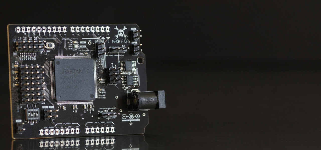
Hacklet 28 – Programmable Logic Hacks posting tells about Arduino-Compatible FPGA Shield. The shield features a Xilinx Spartan 6 FPGA and is available in The Hackaday Store. It has the needed regulators and level shifters. The price is $69.97. Not sure where to start? Check out  Spartan-6 FPGA Hello World! that uses Xilinx’s free tool chain to getting a “hello world” led blinker running!

Hacklet 28 – Programmable Logic Hacks posting also mentions Chameleon. Chameleon is an Arduino compatible FPGA board with a Xilinx Spartan 3A FPGA on-board. The Chameleon Arduino-compatible shield board was designed to support two general application areas: (1) soft-core processors, and (2) intelligent serial communications interface.

Cheap FPGA-based HDMI Experimenting Board project is designing a (relatively) cheap little board for experimenting with HDMI using a Spartan-6 FPGA.

431 Comments

  1. Tomi Engdahl says:

    Does the World Need an FPGA Arduino?
    http://hackaday.com/2016/03/09/does-the-world-need-an-fpga-arduino/

    What would you get it you mashed up an FPGA and an Arduino? An FPGA development board with far too few output pins? Or a board in the form-factor of Arduino that’s impossible to program?

    Fortunately, the ICEZUM Alhambra looks like it’s avoided these pitfalls, at least for the most part. It’s based on the Lattice iCE40 FPGA,

    ICEZUM Alhambra board
    https://github.com/bqlabs/icezum/wiki

    FPGA development board (iCE40HX1K-TQ144 from lattice)
    Open hardware
    Compatible with the opensource icestorm toolchain
    Multiplatform: Linux / Mac / Windows
    Arduino like board: similar pinout than Arduino one / BQ zum.
    You can Reuse most of available Arduino / Zum shields
    Control your robots / printbots from an FPGA
    12 MHZ MEMS oscillator

    Reply
  2. Tomi Engdahl says:

    Resolve picoseconds using FPGA techniques
    http://www.edn.com/design/integrated-circuit-design/4441555/Resolve-picoseconds-using-FPGA-techniques?elqTrackId=15bc7898a9504d0e8dbc593a76429924&elq=aba3f8bcd3764b75912aee5acaf428cf&elqaid=31210&elqat=1&elqCampaignId=27281

    A low area and high stability Time-to-Digital Converter (TDC) circuit implemented with a shifted-clock sampling technique is proposed. It is tested on a Xilinx Virtex-5 ML507 device. The results demonstrate the TDC achieves a dynamic range of 10 µs, 64 ps resolution, differential nonlinearity (DNL) of less than 0.3 LSB, and integral nonlinearity (INL) better than 0.6 LSB.

    Time to digital converters often find use in high energy physical experiments such as exploring subatomic level fine structure in fixed target experiments and collision experiments[1-2], where they need accuracy in the picosecond level. Designs are usually implemented with Application Specific Integrated Circuits (ASICs) for their high precision and stability compared with TDCs implemented on FPGA [3-4]. But TDCs based on FPGA also can reach picosecond precision [5]. TDCs implemented on FPGA need to take important features into consideration: quantization step, measurement range, standard measurement uncertainty, nonlinearities, dead time, and readout speed.

    The simplest design of TDC is the direct counting method, but in this way we only could measure the coarse time intervals between start and stop signals

    There are two schemes used to improve the resolution in the design of TDCs, namely tapped delay line (TDL) and shifted clock sampling (SCS). Both of them interpolate between clocks

    Reply
  3. Tomi Engdahl says:

    Maker Community Takes Up the FPGA
    http://www.eetimes.com/document.asp?doc_id=1329227&

    The powerful but complex field programmable gate array (FPGA), long considered a tool for the technical elite, is unexpectedly finding new popularity in the non-elite world of the maker community.

    Increasingly, suppliers are marketing devices and software to make the FPGA’s tricky implementation more accessible to the masses. New development kits and boards are rolling out, simplifying the complex FPGA programming process and attracting a more technically literate class of “makers.”

    “We’re seeing professional engineers — graduates with master’s degrees and four or five years experience in industry,” Mark Jensen, corporate software strategy and marketing director for Xilinx, Inc., told Design News. “They call themselves Pro Makers. And they see that they can use FPGAs to build programmable robots and drones, then get crowd source funding, and create their own grassroots businesses out of it.”

    The result is an odd convergence: a new class of makers, maybe not formally educated in FPGA programming, but smart enough to apply the new breed of simpler development kits in ways that no one has up to now. Some of the new makers are night owls, breathing life into their ideas when they return from their nine-to-five engineering jobs. Others are students – electrical and mechanical engineers alike – learning the technology while they complete a senior project or master’s thesis. They’re building an unusual assortment of mechanized devices – from self-balancing bicycles to robots that run like cheetahs – and they’re using FPGAs for intelligence.

    “Some of these projects use really complex non-linear control algorithms, so the developers have to use FPGAs to get the performance they need,”

    Reply
  4. Tomi Engdahl says:

    Software-defined FPGA computing with QuickPlay: Product how-to
    http://www.edn.com/design/integrated-circuit-design/4441611/Software-defined-FPGA-computing-with-QuickPlay–Product-how-to?_mc=NL_EDN_EDT_EDN_review_20160318&cid=NL_EDN_EDT_EDN_review_20160318&elqTrackId=aa98994cafb04692a3ef93ca04013218&elq=a31bf67fa4884ef18038368756f62577&elqaid=31389&elqat=1&elqCampaignId=27436

    Data-centre equipment manufacturers have long been keen to take advantage of the massive parallelism possible with FPGAs to achieve the processing performance and I/O bandwidth needed to keep pace with demand, within a highly efficient power budget. Traditionally however, implementing a hardware computing platform in an FPGA has been a complex challenge that has required designers to deal with some of the lowest levels of hardware implementation.

    Although some recent FPGA-design methodologies incorporating High-Level Synthesis (HLS) tools and software programming languages such as OpenCL, C, and C++ have simplified the task, they have not eliminated the need for specialist FPGA-design expertise. There is a need for a high-level workflow that allows software engineers to use an FPGA as a software-defined computing platform without the pain of hardware design. To satisfy this need, such a workflow should be able to:

    Create functional hardware from pure software code
    Incorporate existing hardware IP blocks if needed
    Infer and create all of the support hardware (interfaces, control, clocks, etc.)
    Support the use of commercial, off-the-shelf boards and custom platforms
    Eliminate hardware debug by ensuring generated hardware is correct by construction
    Support debug of functional blocks using standard software debug tools only

    Familiar challenges

    A software developer without specific hardware expertise could generate Kernel 1 and Kernel 2, using a high-level synthesis tool such as Vivado HLS to compile the software functions Function1() and Function2() as written in C or C++ into FPGA hardware descriptions in VHDL or Verilog. However, the non-algorithmic elements of the design, such as interfaces, control, clocks, and resets could not be generated with HLS tools. Hardware designers would be needed to create these as custom IP.

    A new approach

    PLDA Group, a developer of embedded electronic systems and IP, has created QuickPlay to allow software developers to accomplish these tasks, and hence implement applications intended for CPUs, partially or fully, on FPGA hardware. In this software-centric methodology, the designer first develops a C/C++ functional model of the hardware engine, and then verifies the functional model with standard C/C++ debug tools. The target FPGA platform and I/O interfaces (PCIe, Ethernet, DDR, QDR, etc.) are then specified, and finally the hardware engine is compiled and built.

    https://www.quickplay.io/

    QuickPlay is an Open FPGA development platform that exposes a standard C/C++ framework and API allowing developers across the board to build FPGA augmented applications in no time and with no hardware expertise. – See more at: https://www.quickplay.io/#sthash.miEmB8xo.dpuf

    An Open FPGA Development Platform

    The QuickPlay development platform provides the software and hardware infrastructure that enable tight integration between design IP, FPGA hardware, application software and design software, allowing developers to build FPGA enabled applications in record time. To facilitate adoption and enable a strong ecosystem of IP vendors, board vendors, and service providers, QuickPlay was engineered as an open platform that leverages industry standards: C/C++ and HDL for kernel design, AXI4 as the interconnect architecture, YAML, IP-XACT as the component/board description formats and Python as the scripting language.
    - See more at: https://www.quickplay.io/product#sthash.BKiPnFPR.dpuf

    Reply
  5. Tomi Engdahl says:

    Resolve picoseconds using FPGA techniques
    http://www.edn.com/design/integrated-circuit-design/4441555/Resolve-picoseconds-using-FPGA-techniques?_mc=NL_EDN_EDT_EDN_review_20160311&cid=NL_EDN_EDT_EDN_review_20160311&elqTrackId=420ef80730234681ba5a48697a1f7bb5&elq=edb7f6f382274515a39af3649a9c4383&elqaid=31272&elqat=1&elqCampaignId=27344

    A low area and high stability Time-to-Digital Converter (TDC) circuit implemented with a shifted-clock sampling technique is proposed. It is tested on a Xilinx Virtex-5 ML507 device. The results demonstrate the TDC achieves a dynamic range of 10 µs, 64 ps resolution, differential nonlinearity (DNL) of less than 0.3 LSB, and integral nonlinearity (INL) better than 0.6 LSB.

    Reply
  6. Tomi Engdahl says:

    FPGA device density is continuing to grow at approximately 2x per node, which is driving more complex and larger FPGA designs. As the complexity grows, FPGA designers are under increasing pressure to accelerate designs and achieve a faster time to market.

    At every phase, FPGA designers need sophisticated synthesis tools to help automate and accelerate the individual tasks

    Source: https://webinar.techonline.com/1812?keycode=TOL4

    Reply
  7. Tomi Engdahl says:

    FPGA device density is continuing to grow at approximately 2x per node, which is driving more complex and larger FPGA designs. As the complexity grows, FPGA designers are under increasing pressure to accelerate designs and achieve a faster time to market. This is requiring FPGA designers to segment the design process into multiple phases to gain productivity improvements at each phase. These phases include design assembly, initial design bring-up, performance tuning and system debug. At every phase, FPGA designers need sophisticated synthesis tools to help automate and accelerate the individual tasks.

    Source: https://webinar.techonline.com/1812?keycode=TOL4

    Reply
  8. Tomi Engdahl says:

    QuickPlay
    https://www.quickplay.io/product
    An Open FPGA Development Platform

    Reply
  9. Tomi Engdahl says:

    Wearable/wristwatch FPGA devkit
    http://www.edn.com/design/design-tools/development-kits/4441731/Wearable-wristwatch-FPGA-devkit?_mc=NL_EDN_EDT_EDN_today_20160330&cid=NL_EDN_EDT_EDN_today_20160330&elqTrackId=512acaf6b635428f90e1252b0d501cde&elq=29f33448b3fe490295eb34fb82c79c41&elqaid=31596&elqat=1&elqCampaignId=27569

    Lattice Semiconductor’s iCE40 Ultra is a low-power platform in compact wrist watch form factor that supports multiple wearable applications, and a range of hardware features make the platform a fit for almost any consumer wearable device.

    The platform comes with a user guide and demos to help expedite device design: based on the iCE40 Ultra FPGA, it features a large number of sensors and peripherals, making it a compelling platform for the design of a wide array of wearable devices.

    The iCE40 Ultra Wearable Development Platform is available now direct from Lattice at a retail price of $270.
    http://www.latticesemi.com/ultrawearable

    Reply
  10. Tomi Engdahl says:

    Swiss Open-Source Processor Core Ready For IoT
    http://www.eetimes.com/document.asp?doc_id=1329327&

    Researchers at ETH Zurich (Swiss Federal Institute of Technology in Zurich) and the University of Bologna have developed PULPino, an open-source processor optimized for low power consumption and application in wearables and the Internet of Things (IoT).

    Open-source and collaborative development is now standard practise in the software world – Linux being an example. While there have been hardware efforts, such as OpenRISC and Opencores, open-source hardware has gained the most traction at the board level. Examples include Arduino and Raspberry Pi, for which the PCB designs are publicly available. However, the chips on which those boards are based have remained proprietary.

    Now a team led by ETH Professor Luca Benini, has put into the public domain the full design of one of their microprocessor systems, a derivative of the PULP (Parallel ultra low power) project.

    The 32-bit PULPino is designed for battery-powered devices with extremely low energy consumption. The arithmetic instructions are also open source: the scientists made the processor compatible with an open-source instruction set – RISC-V – developed at the University of California in Berkeley

    PULPino is a simplified version of the more general PULP, in that it has a single processing element rather than a cluster of four processing elements and has simplified instruction and data RAMs and was implemented in FPGA in 2015.

    According to presentation materials (downloadable from http://www.pulp-platform.org) the PULPino core is called RI5CY and is a four-stage in-order pipeline implementation of RISC-V.

    The core which is compared to a Cortex-M4 from ARM, has an instructions per cycle figure close to 1, support for the base integer instruction set (RV32I), compressed instructions (RV32C) and partial support for the multiplication instruction set extension (RV32M).

    The PULP quad-core IC was subject of a tape-out in 28nm from Globalfoundries in November 2015 while the first PULPino implementation (called Imperio) taped out in January 2016 in 65nm CMOS from UMC.

    We are happy to share our FREE and OPEN-SOURCE microprocessor system PULPino!
    http://www.pulp-platform.org/

    You can download the entire source code, test programs, programming environment and even the bitstream for the popular ZEDboard, completely for free under the Solderpad license.

    ZedBoard Zynq-7000 ARM/FPGA SoC Development Board
    $495.00
    http://store.digilentinc.com/zedboard-zynq-7000-arm-fpga-soc-development-board/

    Reply
  11. Tomi Engdahl says:

    Cognitive Computing Platform Unites Xilinx and IBM
    http://www.eetimes.com/document.asp?doc_id=1329377&

    Xilinx and IBM announced that they will enable FPGA-based acceleration within the SuperVessel OpenPOWER development cloud services offered on ptopenlab.com.

    SuperVessel is a first-of-its-kind open access cloud service that acts as a virtual R&D engine for application developers, system designers, and academic researchers to create, test and pilot solutions for emerging applications including deep analytics, machine learning and the Internet of Things (IoT).

    The open access cloud service will leverage Xilinx’s SDAccel Development Environment, hosted in SuperVessel, for application developers to describe their algorithms in OpenCL, C, and C++ and compile directly to Xilinx FPGA-based acceleration boards.

    SDAccel Application Development on SuperVessel OpenPOWER Cloud
    http://www.xilinx.com/products/design-tools/software-zone/sdaccel/supervessel.html

    Reply
  12. Tomi Engdahl says:

    A Raspberry Pi In An FPGA
    http://hackaday.com/2016/04/26/a-raspberry-pi-in-an-fpga/

    Somehow or another, the Raspberry Pi has become a standardized form factor for single board computers. There are now Raspberry Pi-shaped objects that can do anything, and between the Odroid and bizarre Intel Atom-powered boards, everything you could ever want is now packaged into something that looks like a Raspberry Pi.

    Except for one thing, of course, and that’s where [antti.lukats]’s entry for the 2016 Hackaday Prize comes in. He’s creating a version of the Raspberry Pi based on a chip that combines a fast ARM processor and an FPGA in one small package. It’s called the ZynqBerry and will, assuredly, become one of the best platforms to learn FPGA trickery on.

    Xilinx’ Zynq comes with a dual-core ARM Cortex A9 running around 1GHZ, and from that fact alone should be about comparable to the original Raspberry Pi.

    ZynqBerry
    Xilinx ZYNQ based RPi
    https://hackaday.io/project/7817-zynqberry

    Reply
  13. Tomi Engdahl says:

    DIPSY
    DIY System on Chip based on FPGA, priced below 5 USD
    https://hackaday.io/project/6592-dipsy

    DIY Yourself System On Chip, at below 5 USD pricing, hacking friendly, small and low power.

    Sized 10x10mm, priced sub 5 USD (BOM price approx 1.5 USD) FPGA Module with ultra low power consumption. Easy accessible 100mil pin header style design.

    Can be used “custom IC” when the FPGA OTP internal NV memory is burned or as coprocessor or accelerator for slow microcontrollers configured over SPI interface.

    NOTE all production documentation and source code in main github repo.
    https://github.com/AnttiLukats/DIPSY

    Reply
  14. Tomi Engdahl says:

    CAT Board
    The CAT Board is part of a Raspberry Pi-based hand-held FPGA programming system.
    https://hackaday.io/project/7982-cat-board

    The CAT Board is an OSHW Raspberry Pi HAT with a Lattice iCE40HX FPGA. It’s meant to be programmed using the OSS myhdl, yosys, arachne-pnr, IceStorm tools right on the RPi.

    Reply
  15. Tomi Engdahl says:

    MCU Guy, Meet FPGA; FPGA, Meet MCU Guy
    http://www.eetimes.com/author.asp?section_id=216&doc_id=1329541&

    If you have heard of FPGAs, Verilog & VHDL, but don’t really know “what lies beneath,” or if you want to introduce someone to FPGA Space, then this column is for you.

    The thing is that I know a lot of MCU-centric guys and gals. Over and over again I hear them say that they’ve heard of FPGAs and they understand that these are devices whose functions can be configured as required, but that’s as much as they know. Similarly, they’ve heard the names Verilog and VHDL — which hardware guys would refer to as hardware description languages (HDLs) — and they know these languages are used to capture the FPGA’s design intent. Once again, however, this is about as far as their knowledge goes.

    All of this explains why I penned a mini-series of articles some time ago

    Reply
  16. Tomi Engdahl says:

    Control an FPGA bus without using the processor
    http://www.edn.com/design/integrated-circuit-design/4441916/Control-an-FPGA-bus-without-using-the-processor?_mc=NL_EDN_EDT_EDN_today_20160503&cid=NL_EDN_EDT_EDN_today_20160503&elqTrackId=144654f1744a4e91a320ebdb744a52c3&elq=3d78c64e58644d598adf09a3fbba33d0&elqaid=32097&elqat=1&elqCampaignId=28017

    Many FPGA designs use an embedded processor for control. A typical solution involves the use of a soft processor such as a Nios, though FPGA SoCs with a built-in hard processor have become popular too.

    These processors greatly simplify the end application, but require a strong programing background and knowledge of complicated toolchains. This can hinder debug, especially if a hardware engineer needs a simple way to read and write to the peripherals without pestering the software engineer.

    This Design Idea uses Altera’s SPI Slave to Avalon MM Bridge to provide a simple way to hop onto the Avalon bus. There are two advantages to this technique: It does not compromise the original system design, and the bridge can co-exist with the embedded processor

    Altera provides a reference design for the SPI-Avalon MM bridge.

    After reverse engineering the Altera example design (the left side of Figure 2), a Python library was developed to create packets that the bridge would accept.

    An example Python script to control the frequency of a digital pattern generator for an LTC1668 DAC is provided in the LinearLabTools Python folder.

    Reply
  17. Tomi Engdahl says:

    Slideshow
    10 Favorite FPGA-Based Prototyping Boards
    http://www.eetimes.com/document.asp?doc_id=1329616&

    Many FPGA development projects end up as custom-designed boards. During the design and development phase, however, using an off-the-shelf development board facilitates hardware-in-the-loop verification and provides for significant risk mitigation of the more challenging technical aspects associated with getting the system up and running.

    We can use these boards for a number of different end applications as such no one board is the magic bullet that enables us to use it for all applications. Each time we come to select a board for our project we must consider not only the performance of the FPGA or as you will see SoC mounted on it but also the types and size of memories available, the interfaces available, such as USB, EIA232, GigE, among others, along with user-accessible IO allowing integration with elements of the application.

    Let us take a look at 10 interesting boards that can be used across a number of different applications.

    Reply
  18. Tomi Engdahl says:

    Design Recipes for FPGAs: Book review
    http://www.edn.com/electronics-products/electronic-product-reviews/other/4442012/Design-Recipes-for-FPGAs–Book-review?_mc=NL_EDN_EDT_EDN_productsandtools_20160516&cid=NL_EDN_EDT_EDN_productsandtools_20160516&elqTrackId=f709a15bc2e94c44beadbbe5b3b20e58&elq=142e18f90fcc490f89513b234b81fa24&elqaid=32274&elqat=1&elqCampaignId=28181

    Peter Wilson’s brand new book Design Recipes for FPGAs is an interesting addition to the writing about FPGAs. At 369 pages it might seem to be the One Real Reference, but in fact it’s more a surf through design examples.

    The examples are given in both VHDL and Verilog, the two most common Hardware Description Languages (HDLs) used in this industry. The book starts with a chapter about the basics of each; VHDL is treated in 16 pages; Verilog in 6. Those amount to about the fastest getting-started guides for any language I’ve seen. And the material is pretty good. It’s far from complete, of course, but will give the novice a grounding in the basics.

    But one warning: HDLs look a lot like a programming language. The last thing you want to think of when working with an HDL is programming. In C and other computer languages statements execute one after another. There’s a flow. That’s mostly absent with an HDL. It’s hardware; everything is happening at the same time (with exceptions).

    FPGA design has a number of steps – the testbench, compilation, synthesis, routing, etc. and Mr. Wilson does take the reader through the design flow. But this is at a very high level. You’ll need additional information to actually create a working FPGA.

    Reply
  19. Tomi Engdahl says:

    Reinventing VHDL Badly
    http://hackaday.com/2016/05/16/reinventing-vhdl-badly/

    A few years ago, Philip Peter started a little pet project. He wanted to build his own processor. This really isn’t out of the ordinary – every few months you’ll find someone with a new project to build a CPU out of relays, logic chips, or bare transistors.

    Search the Internet for some tips and tricks for schematic capture programs like KiCad and Eagle, and you’ll find some terrible design choices. If you want more than one copy of a very specific circuit on your board, you have to copy and paste. Circuit simulation is completely separate from schematic capture and PCB design, and unit testing – making sure the circuit you designed does what it’s supposed to do – is a completely foreign concept. Schematic capture and EDA suites are decades behind the curve compared to even the most minimal software IDE.

    Philip is using Eagle to build his small processor – not that there’s anything wrong with that – but with the choice of EDA suite comes a 30-year history of updates to what is essentially a program written for DOS. That said, Eagle does have a lot of options for scripting common tasks, and combined with a few custom Python scripts to write those Eagle scripts, Phillip managed to do a lot with a little.

    Taking a software development background to schematic capture and board design can go so much further than adding modules and objects to Eagle, though. Test-driven development is where it’s at, and Philip is designing his processor with the belief that eventually, he will mess something up. Software devs are humble like that.

    Philip is relying on SPICE, a simulator for analog hardware, to see if the circuits will pass the unit tests.

    Schematic capture and board design is a very, very hard problem to solve. Eagle has been in development for almost 30 years, and it’s still not ideal. Altium has been around for even longer, and there are still problems and unintuitive ways of doing things. KiCad is still a baby at 25 years old, and the general assumption is that KiCad is getting there, but it isn’t for prime time yet.

    What Philip has done is bring tools and techniques in from the software development world, producing something that is much, much better than what we have now. It’s more abstract, yes, but that’s never stopped anyone from putting enterprise Java on their resume.

    Reply
  20. Tomi Engdahl says:

    Using An FPGA To Generate Ambient Color From Video
    http://hackaday.com/2016/05/20/using-an-fpga-to-generate-ambient-color-from-video/

    We should all be familiar with TV ambient lighting systems such as Philips’ Ambilight, a ring of LED lights around the periphery of a TV that extend the colors at the edge of the screen to the surrounding lighting. [Shiva Rajagopal] was inspired by his tutor to look at the mechanics of generating a more accurate color representation from video frames, and produced a project using an FPGA to perform the task in real-time. It’s not an Ambilight clone, instead it is intended to produce as accurate a color representation as possible to give the impression of a TV being on for security purposes in an otherwise empty house.

    The concern was that simply averaging the pixel color values would deliver a color, but would not necessarily deliver the same color that a human eye would perceive. He goes into detail about the difference between RGB and HSL color spaces

    NTSC and VGA decoding

    Ambient TV Lighting
    A low-power solution for creating ambient light based on a TV signal
    https://people.ece.cornell.edu/land/courses/ece5760/FinalProjects/s2016/svr24/svr24/index.html

    Reply
  21. Tomi Engdahl says:

    Hand Gestures Play Tetris
    http://hackaday.com/2016/05/28/hand-gestures-play-tetris/

    There are reports of a Tetris movie with a sizable budget, and with it come a plentiful amount of questions about how that would work. Who would the characters be? What kind of lines would there be to clear? Whatever the answers, we can all still play the classic game in the meantime. And, thanks to some of the engineering students at Cornell, we could play it without using a controller.

    This hack comes from [Bruce Land]’s FPGA design course. The group’s game uses a video camera which outputs a standard NTSC signal and also does some filtering to detect the user. From there, the user can move their hands to different regions of the screen, which controls the movement of the Tetris pieces. This information is sent across GPIO to another FPGA which uses that to then play the game.

    Hand Motion Controlled Tetris
    https://people.ece.cornell.edu/land/courses/ece5760/FinalProjects/s2016/rjb297_map379_cs795/rjb297_map379_cs795/rjb297_map379_cs795/index.html

    This final project for ECE 5760 takes a very well known and classic game and puts a twist on it. Tetris was released in 1984 and since then has become an iconic game, garnering many reproductions and modifications to the original version. Our version of Tetris aims to produce the original Tetris game using a DE2-115 FPGA from Altera. Using VGA as an output and a camera that is able to detect skin tone, the user can play the game using motions that are sensed from their hand. There are four main regions of the screen. These regions control whether the block moves right, left, rotates, or moves down twice as fast. By filtering the video stream and looking for specific types of color in the YUV color space, the hardware recognizes when a user’s hand goes into one of the four sections and sends a signal to the game, instructing it what to do with the block.

    Reply
  22. Tomi Engdahl says:

    10 Favorite FPGA-Based Prototyping Boards
    http://www.eetimes.com/document.asp?doc_id=1329616&

    Many FPGA development projects end up as custom-designed boards. During the design and development phase, however, using an off-the-shelf development board facilitates hardware-in-the-loop verification and provides for significant risk mitigation of the more challenging technical aspects associated with getting the system up and running.

    Each time we come to select a board for our project we must consider not only the performance of the FPGA or as you will see SoC mounted on it but also the types and size of memories available, the interfaces available, such as USB, EIA232, GigE, among others, along with user-accessible IO allowing integration with elements of the application.

    Let us take a look at 10 interesting boards

    Reply
  23. Tomi Engdahl says:

    Real-Time FPGA Finger Detection
    http://hackaday.com/2016/06/04/real-time-fpga-finger-detection/

    The student projects that come out of [Bruce Land]’s microcontroller- and FPGA-programming classes feature here a lot, simple because some of them are amazing, but also because each project is a building-block for another. And we hope they will be for you.

    This time around, [Junyin Chen] and [Ziqi Yang] created a five-in-a-row video game that is controlled by a pointing finger. A camera, pointed at the screen, films the player’s hand and passes the VGA data to an FPGA. And that’s where things get interesting.

    An algorithm in the FPGA detects skin color and, after a few opening and closing operations, comes up with a pretty good outline of the hand. The fingertip localization is pretty clever. They sum up the number of detected pixels in the X- and Y-axis, and since a point finger is long and thin, locate the tip because it’s going to have a maximum value in one axis and a minimum along the other.

    Pseudo Touch Screen Game
    Camera Based Finger Detection
    https://people.ece.cornell.edu/land/courses/ece5760/FinalProjects/s2016/jc2954_zy259/jc2954_zy259/jc2954_zy259.html

    Reply
  24. Tomi Engdahl says:

    FPGA-and-Pi Colossus Smashes Your Codes!
    http://hackaday.com/2016/06/08/fpga-and-pi-colossus-smashes-your-codes/

    If it were sixty years ago, and you were trying to keep a secret, you’d be justifiably glad that [Ben North] hadn’t traveled back in time with his Raspberry-Pi-and-FPGA code-breaking machine.

    [Ben]’s build combines his explorations into old-school cryptanalysis with a practical learning project for FPGAs. If you’re interested in either of the above, give it a look. You can start out with his Python implementations of Colossus to get your foot in the door, and then move on to his GitHub repository for the FPGA nitty-gritty.

    It’s also a cool example of a use for the XuLA2 FPGA board and its companion StickIt board that plug straight into a Raspberry Pi for programming and support.

    (Some of) Colossus in an FPGA
    http://bennorth.github.io/fpga-colossus/doc/Content/notes.html

    Reply
  25. Tomi Engdahl says:

    XuLA2-LX25
    http://www.xess.com/shop/product/xula2-lx25/

    Open-source design
    XC6SLX25 FPGA
    32 MByte SDRAM
    8 Mbit Flash
    microSD card socket
    3.3 & 1.2V regulators
    40-pin interface
    12 MHz oscillator
    PIC 18F14K50 micro
    USB 2.0 port
    Auxiliary JTAG port
    Works with the XSTOOLs software
    Works with XILINX ISE and WebPACK
    Works with XILINX iMPACT and ChipScope (requires Xilinx JTAG cable)

    $119.00

    Reply
  26. Tomi Engdahl says:

    Smart FPGA Debugging Tools Reduce Validation Times
    http://www.eetimes.com/author.asp?section_id=36&doc_id=1329879&

    Designers who focus more heavily on an FPGA’s debug capabilities before they select their next device can reduce development cycles and costs while significantly speeding time to market.

    FPGA and SoC designers face many challenges to get their product into production. Typically, they start by evaluating the appropriate device for their design; then they implement the hardware description language (HDL) design, fit the device, and — finally — debug the entire FPGA before it can be brought into production.

    The reality today is that, for many designs, particularly those in the industrial and embedded markets, any number of FPGAs will work. In most cases, the decision as to which FPGA vendor to choose comes down to experience with the development software.

    Debug basics — logic analyzers
    Every major FPGA vendor offers a logic analyzer as a debug tool. This is a technique that uses internal FPGA logic elements and embedded block memory to implement functions. A designer can specify which signals to monitor and set up a trigger to tell the logic analyzer when to start capturing data.

    It is important to note that, because these signals need to be sampled, they are not capturing the real-time performance of the data.

    Next-generation debug tools
    Because of the limitations of logic analyzers for debugging, new debug tools have been designed to speed up FPGA and board validation. Some EDA vendors are offering tools that integrate logic analyzer functionality into the synthesis tool to shorten the iteration of bug finding. When the logic analyzer is integrated with the synthesis tool, this allows technology views into the design and easier trigger setup. A designer can also make design changes and have them automatically mapped back to the register transfer level (RTL) code.

    FPGA designers typically spend about 30 percent or more of their time in debug. This percentage could go even higher depending on the size and state of the project. Debugging can be painful because it involves many iterative cycles with limited observability and controllability, frequent re-runs of place-and-route, timing closure, and re-programming. By leveraging smart debugging tools, engineers can validate their FPGA designs much faster than just using a traditional inserted logic analyzer.

    Enhanced debug capabilities are a game-changing development for FPGA designers.

    Reply
  27. Tomi Engdahl says:

    10 Ways To Program Your FPGA
    http://www.eetimes.com/document.asp?doc_id=1329857&

    Despite the recent push toward high level synthesis (HLS), hardware description languages (HDLs) remain king in field programmable gate array (FPGA) development. Specifically, two FPGA design languages have been used by most developers: VHDL and Verilog. Both of these “standard” HDLs emerged in the 1980s, initially intended only to describe and simulate the behavior of the circuit, not implement it.

    However, if you can describe and simulate, it’s not long before you want to turn those descriptions into physical gates.

    For the last 20 plus years most designs have been developed using one or the other of these languages, with some quite nasty and costly language wars fought. Other options rather than these two languages exist for programming your FPGA. Let’s take a look at what other tools we can use.

    C / C++ / System C

    The C, C++ or System C option allows us to leverage the capabilities of the largest devices while still achieving a semblance of a realistic development schedule… although that may just be my engineering management side coming out.
    The ability to use C-based languages for FPGA design is brought about by HLS (high level synthesis), which has been on the verge of a breakthrough now for many years
    Recently it has become a reality with both major vendors, Altera and Xilinx offering HLS within their toolsets Spectra-Q and Vivado HLx respectively.
    A number of other C-based implementations are available, such as OpenCL which is designed for software engineers who want to achieve performance boosts by using a FPGA without a deep understanding of FPGA design. Whereas HLS is still very much in the area of FPGA engineers who want to increase productivity.

    MyHDL

    MyHDL is a python package that enables us to use python to design our FPGA; what’s more, it is open source and freely available. It is not however an HLS tool, so the developer still needs to understand FPGA design techniques.
    Most algorithms implemented in FPGA start out at a high level using floating point numbers. MyHDL allows you to use the same language for the algorithm development as for your implementation.
    To achieve concurrency, MyHDL uses generators, and communication between concurrent modules uses an object called a signal, which is within the MyHDL package.
    MyHDL is interesting because it provides for a potentially powerful simulation environment by leveraging the power of the wider python language to generate test benches and stimulus. This includes native support for databases, GUI’s and so on. MyHDL is supplied with its own simulation tool.
    Despite using python, it is not a high level synthesis tool: As such, the resultant code is still at a relatively low level

    CHISEL

    CHISEL, an acronym like VHDL, it actually stands for Constructing Hardware In a Scala Embedded language. It is another open-source language and was developed at UC Berkeley, the same university that gave us SPICE.
    Within the FPGA world, we use CHISEL very similarly to MyHDL although there are some subtle differences: The first being that CHISEL is object orientated, the second is in how we verify and use our CHISEL design.
    CHISEL outputs a Verilog for hardware implementation and C++, with the C++ being used for verification with a software model.

    JHDL

    Just another (JAVA) Hardware Description Language is also another academically generated language
    Differing from MyHDL and CHISEL, the output from JHDL is an EDIF netlist, this traditionally generated post synthesis.
    development of JHDL appears to have stopped, it has led to the development of RapidSmith

    BSV

    BSV (Bluespec SystemVerilog) is a language developed by Bluespec Inc and is based around Haskell. This language is designed to be used with the Bluespec compiler (BSC), which is an HLS compiler. The BSC generates either synthesizable Verilog or executable System C.

    MATLAB

    This is one language that every FPGA engineer should be familiar with from university and the field of work. We use MATLAB to generate filters for signal processing, develop image processing algorithms and almost any other algorithm. It is however possible to go from MATLAB model to FPGA using the HDL coder. What makes it even more impressive is traceability is maintained as such that high integrity applications can be developed using this approach.
    Like many of the languages mentioned here, HDL coder outputs either synthesizable VHDL or Verilog that you can implement within your FPGA development flow.

    LabVIEW FPGA

    The LabVIEW frame work gives you a totally different way of programming your FPGA. For those unfamiliar with LabVIEW, it is a graphical language (actually called “G”). The catch with developing FPGAs using LabVIEW FPGA: You need to develop using specific hardware from National Instruments called Reconfigurable IO (RIO for short) modules. These modules are based around Xilinx FPGAs with the latest one being the Zynq.

    SystemVerilog

    A logical extension of the Verilog language combined with OpenVera and SuperLog languages, SystemVerilog has led to what has been called the first hardware design and verification language. That is, we can use SystemVerilog for developing the RTL for the FPGA, or we can use it for verification—an arena where it is very powerful.
    builds upon the traditional Verilog language
    SystemVerilog greatly differs from Verilog, however, in that SystemVerilog supports an object-orientated programming.

    VHDL / VERILOG

    VHDL and VERILOG are the current staples of FPGA design, both having been developed in the 1980s. VHDL stems from the US Department of Defense and Verilog from the commercial sector.
    Both languages provide structures to describe the inherently parallel nature of FPGA / ASIC development.
    Over the years, both languages have had a number of updates
    With the increases in device size and complexity over the last few years, the days of these traditional HDLs may be declining.
    However, I cannot see them being fully replaced in the immediate short term

    SPINAL HDL

    Again this language, like many of the ones presented here, outputs a VHDL file that is used in your simulation and synthesis tools. It does come with a development IDE
    It appears to be very similar to CHISEL being both object orientated and based upon SCALA.
    includes support using existing VHDL and Verilog IP.

    Reply
  28. Tomi Engdahl says:

    FPGA Powers Blazingly Fast LED Matrix Audio Visualizer
    http://hackaday.com/2016/06/13/fpga-powers-blazingly-fast-led-matrix-audio-visualizer/

    [Sam Miller], [Sahil Gupta], and [Mashrur Mohiuddin] worked together on a very fast LED matrix display for their final project in ECE 5760 at Cornell University.

    They started, as any good engineering students, by finding a way to make their lives easier. [Sam] had built a 32×32 LED matrix for another class. So, they made three more and ended up with a larger and more impressive 64×64 LED display.

    The brains of the display is an Altera DE2-115 FPGA board. The code is all pure Verilog. The FFT and LED control are implemented in hardware on the FPGA; none of that Altera core stuff. To generate images and patterns they wrote a series of python scripts.

    The team has promised to upload all the code to GitHub:

    LED Matrix Visualizer
    Verilog project to control a 64×64 LED matrix and respond to music. Final project for the Cornell University course ECE5760 taught by Bruce Land.
    https://github.com/sm11963/led-matrix-visualizer

    ECE 5760: Final Project
    RGB LED Matrix Audio Visualizer
    https://people.ece.cornell.edu/land/courses/ece5760/FinalProjects/s2016/sgm82_skg73_mm889/sgm82_skg73_mm889/sgm82_skg73_mm889/index.html

    The system was controlled completely using Altera’s DE2-115 FPGA. Music was read into the FPGA through its Line In port and internal ADC from which the audio was processed and output from the Line Out Port. While a VGA was used for initial testing of the visualizer, the final output was wired to the LED Matrix via the FPGA’s 40-pin GPIO connection.

    The LEDMatrix module is used to interface with the LEDMatrix display hardware through the GPIO pins. It exposes an interface to connect to two RAM buffers and then write out to the GPIO pins.

    Reply
  29. Tomi Engdahl says:

    No Frame Buffer for FPGA VGA Graphics
    http://hackaday.com/2016/06/16/no-frame-buffer-for-fpga-vga-graphics/

    Usually, when you think of driving a VGA–in software or hardware–you think of using a frame buffer. The frame buffer is usually dual port RAM. One hardware or software process fills in the RAM and another process pulls the data out at the right rate and sends it to the VGA display (usually through a digital to analog converter).

    [Connor Archard] and [Noah Levy] wanted to do some music processing with a DE2-115 FPGA board. To drive the VGA display, they took a novel approach. Instead of a frame buffer, they use the FPGA to compute each pixel’s data in real-time.

    The FPGA can track up to 64 objects on the screen at a time including depth.

    https://people.ece.cornell.edu/land/courses/ece5760/FinalProjects/s2016/cwa37_nml45/cwa37_nml45/cwa37_nml45/index.html

    Reply
  30. Tomi Engdahl says:

    Recreating Chiptunes In Verilog
    http://hackaday.com/2016/06/19/recreating-chiptunes-in-verilog/

    The semester is wrapping up at Cornell, and that means it’s time for the final projects from [Bruce Land]’s lab. Every year we see some very cool projects, and this year is no exception. For their project, [Andre] and [Scott] implemented the audio processing unit (APU) of the Nintendo Entertainment System (NES). This is the classic chiptune sound that regaled a generation with 8-bit sounds that aren’t really eight bits, with the help of a 6502 CPU that isn’t really a 6502 CPU.

    Unlike the contemporaneous MOS 6581 SID, which is basically an analog synthesizer on a chip, the APU in the NES is extraordinarily spartan. There are two pulse wave channels, a triangle wave channel, a random noise channel, and the very rarely used delta modulation channel (DMC) used to play very low quality audio samples. This is a re-implementation of the NES APU for a university lab; it is very understandable that [Andre] and [Scott] didn’t implement the rarely used DMC.

    ece5760 Final Project:
    NES Music Player
    https://people.ece.cornell.edu/land/courses/ece5760/FinalProjects/s2016/avh34_sz296/ece5760_Final_Project_avh34_sz296/ece5760_Final_Project_avh34_sz296/ece5760.Final.Project.Report/ece5760.Final.Project.Report.html

    Reply
  31. Tomi Engdahl says:

    Mag Lev Without The Train (But With An FPGA)
    http://hackaday.com/2016/06/26/mag-lev-without-the-train-but-with-an-fpga/

    Some students at Cornell University decided to implement the control loop to produce levitation using an Altera FPGA. An inductive sensor determined the position of an iron ball. The device uses a standard proportional integral derivative (PID) control loop. The control loop and PWM generation occur in the FPGA hardware. You can see a video of their result

    the device has an embedded NIOS II processor core that handles tasks including displaying data and changing PID constants

    This project is a good example of marrying FPGA logic for high speed and a CPU for easier development.

    FPGA controlled Magnetic Levitation
    https://people.ece.cornell.edu/land/courses/ece5760/FinalProjects/s2016/crl233_gp348_nds55/gp348_crl233_nds55/gp348_crl233_nds55/index.html

    Reply
  32. Tomi Engdahl says:

    If You Could Have the Ideal Programmable Logic Device, What Would it Be?
    http://www.eetimes.com/author.asp?section_id=28&doc_id=1329998&

    An FPGA advert from 30 years ago really emphasizes the tremendous strides that have been made in programmable logic technology.

    in the May 29, 1986 issue of EDN announcing the availability of the XC-2064 Logic Cell Array. At that time, if you wanted custom logic in your design, you really had only two options — simple programmable logic devices (PLDs) like PROMs at one end of the spectrum and the Gate Array (GA) class of Application-Specific Integrated Circuits (ASICs) at the other. (The moniker “Logic Cell Array” was intended to contrast with “Gate Array” — over time this would transition into the Field-Programmable Gate Array (FPGA) appellation we know and love today).

    The XC-2064 comprised an 8 x 8 = 64 array of Logic Cells, each containing a 4-bit lookup table (LUT) and a flip-flop, along with 38 GPIOs. That was it. There wasn’t even any RAM.

    On the bright side, there was sophisticated (for the time) development software available.

    . The problem at that time was that PLDs were cheap and they were a known quantity. Also, their input-to-output timing was deterministic (it was specified in the datasheet); by comparison, the XC-2064′s timing depended on how you partitioned your logic into the LUTs and how you routed the LUTs together.

    Who could have imagined that FPGAs would evolve from that cuddly little rascal to today’s behemoths with their multi-hundred-megahertz clocks, multi-hundred-megabit RAMs, hundreds of thousands of LUTs, thousands of DSP blocks, thousands of GPIOs, embedded processor cores, high-speed transceivers… the list goes on.

    Reply
  33. Tomi Engdahl says:

    Emulating A Remote Control Ceiling Fan Transmitter In An FPGA
    http://hackaday.com/2016/07/04/emulating-a-remote-control-ceiling-fan-transmitter-in-an-fpga/

    [Joel] has a remote control ceiling fan. It’s nothing special, the controller has a low-power 350MHz transmitter and a Holtek encoder to send commands by keying the transmitter’s output. Desiring something a little better, he set about reverse engineering the device’s protocol and implementing it on a Lattice iCE40 FPGA.

    To decode the device’s packets he reached for his RTL-SDR receiver and took a look at it in software. GQRX confirmed the presence of the carrier and allowed him to record a raw I/Q file, which he could then supply to Inspectrum to analyse the packet structure. He found it to be a simple on-off keying scheme, with bits expressed through differing pulse widths. He was then able to create a Gnu Radio project to read and decode them in real time.

    350MHz FPGA Ceiling Fan Remote
    https://airwebreathe.org.uk/doku.php?id=350mhz_fpga_ceiling_fan_remote

    Reply
  34. Tomi Engdahl says:

    FPGA constraints for the modern world: Product how-to
    http://www.edn.com/design/integrated-circuit-design/4442317/FPGA-Constraints-for-the-modern-world–Product-how-to?_mc=NL_EDN_EDT_EDN_today_20160705&cid=NL_EDN_EDT_EDN_today_20160705&elqTrackId=55068d5a4c444b1e858e60a0efd4ec50&elq=ea3cd78c37fc481dbd2eaea7b34d6afe&elqaid=32939&elqat=1&elqCampaignId=28766

    Today’s FPGAs are larger and more complex than ever, and defining and applying correct design constraints is one of the biggest challenges. When the design fails to meet the timing performance requirements it can be very time consuming to find the issues, but the process is made easier with well-defined constraints.

    Constraint setup can be a daunting task, and synthesis tools such as Synopsys’ Synplify Pro and Premier can help with automatic template creation, “autoconstraining” of new designs, setup and import of IP-specific constraints, and forward annotation to place and route software.

    This articles details how Synplify, a timing-driven synthesis tool, enables designers to develop and apply correct timing constraints to achieve good quality of results (QoR). The following are the design elements that FPGA designers should consider when developing constraints:

    Identify clocks
    Identify and creating clock groupings and clock relationships
    Constrain clocks
    Constrain inputs and outputs
    Define multi-cycle paths and false-paths

    Initial setup and identification of clocks

    When starting a new project, designers need to setup the environment and define the overall input for the design.

    Reply
  35. Tomi Engdahl says:

    Lightweight Game Console Packs a Punch
    http://hackaday.com/2016/07/13/lightweight-game-console-packs-a-punch/

    [Fotino] wrote his own compiler in C++ that converts from C-like languages to a custom-designed assembler that he has dubbed Consolite Assembly. To test his code, he also wrote an emulator before loading it onto the Mimas V2 FPGA board. Presently, Consolite uses 64KiB of main memory and 48 KiB of video memory

    An SD card functions as persistent storage for up to 256 programs, which can be accessed using the hardware switches on the Mimas

    Not wanting for diligence, [Fotino] has provided thorough documentation of nearly every step along the way in his blog posts and on GitHub

    Consolite, a Tiny Game Console on an FPGA
    https://fotino.me/consolite-fpga/

    If you wish to make a game from scratch, you must first invent the universe.

    For my latest project, I am diving back into Verilog to create the hardware side of Consolite. For those who don’t know, Consolite is the name I’ve given to my design of a tiny hobbyist game console and associated software toolchain. In my previous posts, I demoed a compiler that translates from a flavor of C to Consolite Assembly, an assembler that translates from Consolite Assembly to binary files, and an emulator that runs the resulting binaries.

    In order to “complete the stack” in some sense, the last thing to do was to implement the console on an FPGA. I also wrote a multiplayer Tron light cycle game to check my work, which turned out to be a lot of fun especially since I ended up adding support for multiple SNES controllers. At the end of this post I’ve added a video of the system in action, as well as an embedded emulator so that you can play Tron in your browser!

    Reply
  36. Tomi Engdahl says:

    STM32 and FPGAs In A Tiny Package
    http://hackaday.com/2016/07/11/stm32-and-fpgas-in-a-tiny-package/

    Slowly, very slowly, the time when we don’t subject embedded beginners to AVRs and PICs is coming. At a glacial pace, FPGA development platforms are becoming ever more capable and less expensive. [Eric Brombaugh] has been playing around with both ARMs and FPGAs for a while now and decided to combine these two loves into a single board that’s capable of a lot.

    This board is fittingly called an STM32F303 + ice5 development board, and does exactly what it says on the tin. There’s an STM32F303 on board providing a 32-bit CPU running at 72 MHz, 48 kB of SRAM, a quarter meg of Flash, and enough peripherals to keep anyone happy. The FPGA side of this board is a Lattice iCE5 with about 3k Look Up Tables (LUTs), and one time programmable non-volatile config memory.

    STM32F303 + ice5 Development Board
    http://ebrombaugh.studionebula.com/embedded/f303_ice5/

    Reply
  37. Tomi Engdahl says:

    FPGA Drives Old Laptop Screen
    http://hackaday.com/2016/07/27/fpga-drives-old-laptop-screen/

    Every year, new models of laptops arrive on the shelves. This means that old laptops usually end up in landfills, which isn’t exactly ideal. If you don’t want to waste an old or obsolete laptop, though, there’s a way to reuse at least the screen out of one. Simply grab an FPGA off the shelf and get to work.

    [Martin] shows us all how to perform this feat on our own, and goes into great detail about how all of the electronics involved work. Once everything was disassembled and the FPGA was wired up, it took him a substantial amount of time just to turn the display on. From there it was all downhill: [Martin] can now get any pattern to show up on the screen, within reason. The only limit to his display now seems to be the lack of external RAM. He currently uses the setup to drive an impressive-looking clock.

    LVDS LCD Hacking
    http://www.martinhubacek.cz/fpga/lvds-lcd-hacking

    Reply
  38. Tomi Engdahl says:

    Manipulators get a 1000x FPGA-based speed bump
    http://hackaday.com/2016/07/23/manipulators-get-a-1000x-fpga-based-speed-bump/

    Robots have been lurching along pretty slowly for a while until recently when researchers at Duke University [PDF] pushed much of the computation to hardware on an FPGA. The result? Path planning in hardware with a 6-degree-of-freedom arm takes under a millisecond to compute!

    http://spectrum.ieee.org/automaton/robotics/robotics-software/custom-processor-speeds-up-robot-motion-planning-by-factor-of-1000

    Reply
  39. Tomi Engdahl says:

    The Perfect Storm: Open ARM + FPGA Board
    http://hackaday.com/2016/08/03/the-perfect-storm-open-arm-fpga-board/

    Playing around with FPGAs used to be a daunting prospect. You had to fork out a hundred bucks or so for a development kit, sign the Devil’s bargain to get your hands on a toolchain, and only then can you start learning. In the last few years, a number of forces have converged to bring the FPGA experience within the reach of even the cheapest and most principled open-source hacker.

    [Ken Boak] and [Alan Wood] put together a no-nonsense FPGA board with the goal of getting the price under $30. They basically took a Lattice iCE40HX4K, an STMF103 ARM Cortex-M3 microcontroller, some SRAM, and put it all together on a single board.

    The Lattice part is a natural choice because the IceStorm project created a full open-source toolchain for it.

    A Perfect Storm
    https://folknologylabs.wordpress.com/2016/07/21/a-perfect-storm/

    myStorm is the perfect combination of a $5 Raspberry Pi Zero, a $1, 32-bit ARM microcontroller and a $5 versatile low power FPGA – an open hardware platform – brought to life with innovative open source software.

    As a low cost development platform for digital devices based on FPGA and ARM technology, myStorm aims to achieve a price point, previously unavailable in FPGA boards.
    Aimed at Engineers, Hobbyists and Students of Electronics and Computing Science, myStorm offers a versatile FPGA platform that can be used as a system building block within physical computing devices.

    Project IceStorm
    http://www.clifford.at/icestorm/

    Reply
  40. Tomi Engdahl says:

    DEF CON: BSODomizing In High Definition
    http://hackaday.com/2016/08/06/def-con-bsodomizing-in-high-definition/

    A few years ago, [Kingpin] a.k.a. [Joe Grand] (A judge for the 2014 Hackaday Prize) designed the most beautiful electronic prank ever. The BSODomizer is a simple device with a pass-through connection for a VGA display and an infrared receiver.

    The original BSODomizer is getting a little long in the tooth. VGA is finally dead.

    HDMI is the future, and FPGAs have never been more accessible. F

    Before simply deciding to add HDMI to the original BSODomizer, [Kingpin] and [Zoz] did the smart thing and figured out what the features of this new, updated display prank toy would be. Full color 1080p was a must, images should be loadable from an SD card, and animations would be a cool feature. That SD card opens up a few possibilities, so they’re also looking into taking screencaps, giving the BSODomizer HD pentesting capabilities far beyond what the original could attain. These features meant an FPGA would be needed.

    The development board chosen for the prototype of the BSODomizer HD was a Cyclone V GX development board, available from the usual retailers for about $170. To this, the team added an HDMI transceiver from Analog. After that, it was only a matter of learning Verilog, FPGA development, and pushing pixels to the screen.

    After creating a few test patterns, the next step was pushing an image over a HDMI cable. A 1920×1080 image at 24bbp is almost six Megabytes, which means some fast memory is needed

    In keeping with the recent DEF CON tradition, this project was more of an introduction to a technique, in this case HDMI and programmable logic. Elsewhere on the Internet, people have been putting together cooler FPGA and HDMI mashups for years, including overlaying video on encrypted HDMI streams, and various ambilight clones that look at pixels before passing them through to a HDMI out port

    http://www.analog.com/en/products/audio-video/analoghdmidvi-interfaces/analog-hdmidvi-display-interfaces/adv7513.html#product-overview

    Reply
  41. Tomi Engdahl says:

    Overlaying video on encrypted HDMI connections
    http://hackaday.com/2012/01/21/overlaying-video-on-encrypted-hdmi-connections/

    [bunnie] is up to his old tricks again. He successfully implemented a man-in-the-middle attack on HDCP-secured connections to overlay video in any HDMI video stream. There’s a bonus, too: his hack doesn’t use the HDCP master-key. It doesn’t violate the DMCA at all.

    The build uses the NeTV, a handy and cheap FPGA board with an HDMI input and output. [bunnie] got the FPGA to snoop the HDMI bus and decide if a pixel needs to be changed or not.

    Reply
  42. Tomi Engdahl says:

    FPGA Based Ambilight Clone
    http://hackaday.com/2015/04/25/fpga-based-ambilight-clone/

    The Philips Ambilight – a bunch of rear-facing RGB LEDs taped to the back of a TV – is becoming the standard project for anyone beginning to tinker with FPGAs. [DrX]’s is the best one we’ve seen yet, with a single board that reads and HDMI stream, makes blinkey lights go, and outputs the HDMI stream to the TV or monitor.

    [DrX] is using an FPGA development board with two HDMI connectors – the Scarab miniSpartan6+ – and a strand of WS2801 individually addressable RGB LEDs for this project. With a bit of level shifting, driving the LEDs was easily taken care of. But what about decoding HDMI?

    Reply
  43. Tomi Engdahl says:

    FPGA constraints for the modern world: Product how-to
    http://www.edn.com/design/integrated-circuit-design/4442317/FPGA-Constraints-for-the-modern-world–Product-how-to?_mc=NL_EDN_EDT_EDN_today_20160713&cid=NL_EDN_EDT_EDN_today_20160713&elqTrackId=891401ad18954eaf863411dfd309b8f3&elq=183f8c45a0d54dcaaf332a5c0cfea6b3&elqaid=33057&elqat=1&elqCampaignId=28885

    Today’s FPGAs are larger and more complex than ever, and defining and applying correct design constraints is one of the biggest challenges. When the design fails to meet the timing performance requirements it can be very time consuming to find the issues, but the process is made easier with well-defined constraints.

    Constraint setup can be a daunting task, and synthesis tools such as Synopsys’ Synplify Pro and Premier can help with automatic template creation, “autoconstraining” of new designs, setup and import of IP-specific constraints, and forward annotation to place and route software.

    This articles details how Synplify, a timing-driven synthesis tool, enables designers to develop and apply correct timing constraints to achieve good quality of results (QoR). The following are the design elements that FPGA designers should consider when developing constraints:

    Identify clocks
    Identify and creating clock groupings and clock relationships
    Constrain clocks
    Constrain inputs and outputs
    Define multi-cycle paths and false-paths

    What constraints are needed?

    In general, FPGA designers need to define the clocks, IP & black boxes, and all other constraints like I/O.

    When starting a new project, designers need to setup the environment and define the overall input for the design.

    Reply
  44. Tomi Engdahl says:

    FPGAs solve challenges at the core of IoT implementation
    http://www.edn.com/electronics-blogs/eye-on-iot-/4442318/FPGAs-solve-challenges-at-the-core-of-IoT-implementation?_mc=NL_EDN_EDT_EDN_review_20160708&cid=NL_EDN_EDT_EDN_review_20160708&elqTrackId=a3622ca5294c436bbb194ce2f1e12343&elq=5911f418b2904351a28495d785d6df64&elqaid=33011&elqat=1&elqCampaignId=28834

    But to reach the tens of billions of devices projected to make up the IoT, designers will have to overcome significant implementation challenges. Some of the key among them will be making IoT devices power efficient, handling incompatible interfaces, and providing a processing growth path to handle the inevitable increase in device performance requirements. An FPGA-based design approach can help address such challenges.

    Reply
  45. Tomi Engdahl says:

    Slideshow
    10 FPGA Design Techniques You Should Know
    http://www.eetimes.com/document.asp?doc_id=1330128&

    Regardless of whether you are using VHDL, System Verilog, or a different design capture language (see also 10 Ways to Program Your FPGA), there are a number of universal design techniques with which FPGA engineers should be familiar, from the very simple to the most advanced.

    Reply
  46. Tomi Engdahl says:

    ‘FleaFPGA Ohm’ Development Board
    https://hackaday.io/project/13048-fleafpga-ohm-development-board

    My own raspi-zero style board, based on the new ECP5 series FPGA from Lattice Semiconductor! ;-)

    FleaFPGA Ohm/Ohm+ are my own attempts at making a powerful FPGA-based development board in a raspi zero form-factor. This time however, I use the new ECP5 FPGA from Lattice Semiconductor! ;-)

    From there on, I decided I wanted to do an all-FPGA variant that was compatible to the pi in terms of GPIO but with ‘a few extras here and there’. I then saw Lattice Semiconductor’s newest ECP5 series FPGA (and far more capable than the MachXO2) became available recently, so I thought what the hey and had a crack at it! :)

    Reply
  47. Tomi Engdahl says:

    FPGA Prototyping Gains Ground
    http://semiengineering.com/fpga-prototyping-gains-ground/

    The popular design methodology enables more sophisticated hardware/software verification before first silicon becomes available.

    FPGA technology for design prototypes is making new inroads as demands increase for better integration between hardware and software.

    FPGA prototyping, also known as physical prototyping, has been supported by all of the major EDA players for some time, and it has been considered an essential tool for the largest chipmakers, along with emulation and simulation. But its reach is growing, spurred by the Internet of Things (IoT), a variety of new markets, and most importantly the tighter connection that exists between hardware and software in sophisticated chips, which can have a significant impact on power and performance.

    Still, FPGA prototyping isn’t always user-friendly. It’s difficult to work with, particularly when it comes to partitioning. And while the technology is fast, it has limits.

    Reply
  48. Tomi Engdahl says:

    ‘Flea Ohm’ FPGA Project
    My own raspi-zero style board, based on the new ECP5 series FPGA from Lattice Semiconductor! ;-)
    https://hackaday.io/project/13048-flea-ohm-fpga-project

    FleaFPGA Ohm/Ohm+ are my own attempts at making a powerful FPGA-based development board in a raspi zero form-factor. This time however, I use the new ECP5 FPGA from Lattice Semiconductor! ;-)

    Reply

Leave a Comment

Your email address will not be published. Required fields are marked *

*

*