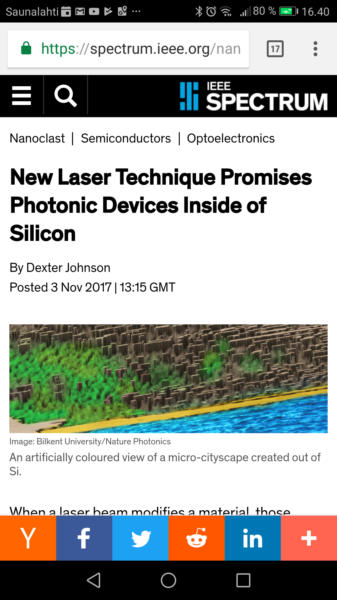
When a laser beam modifies a material, those modifications can either be temporary or permanent, and the change can also be either extremely subtle or drastic. The modified material starts responding differently to the laser beam. Scientists have taken advantage of these interactions to create structures within silicon that enable photonic devices.
“We can also imagine hybrid-systems, with in-chip photonics integrated to electronics and microfluidics parts, thus complementing them. These can incorporate waveguides for data transfer, holograms for diffractive optics, and other microparts to realize advanced biosensors, when coupled with meandering networks of channels.”
0 Comments
Be the first to post a comment.