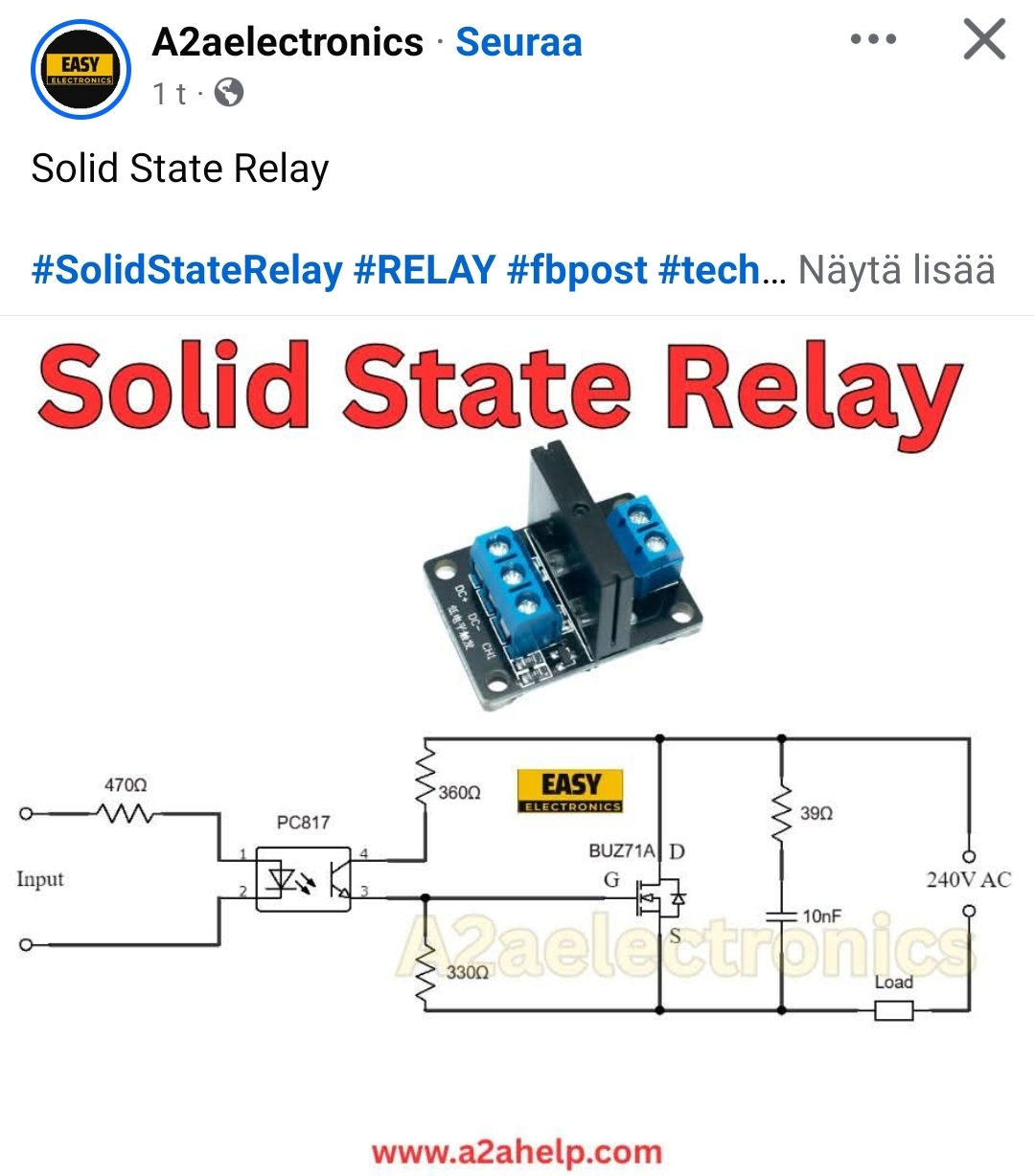
I saw this bad circuit posted to Facebook:
It at quick glance looks like a FET based solid state relay (SSR) design to control 230V AC. But actually it is not suitable for the application at all. If you connect the circuit like shown, it will not work as planned and many components will be fried. This circuit cannot operate at a voltage of 230 V.
The BUZ71A transistor is controlled by the gate voltage only when the collector-emitter voltage is positive. In the negative half of the sine wave, this transistor behaves as a forward diode. The BUZ 71A has a reverse diode, which means it will always pass the negative phase of mains voltage no matter if there is drive voltage on the gate or not.
Starting from the fact that BUZ 71A has max drain source voltage 50 V. When a MOSFET is turned off, an avalanche breakdown occurs if the voltage applied between the drain and source exceeds the absolute maximum rating VDSS that is here 50V. The BUZ 71A will see peak voltage up to slightly over 320V.
The BUZ 71A N-channel power MOSFET has a maximum gate-source voltage (Vgs) of +/- 20V. This means the voltage applied between the gate and source terminals should not exceed 20 volts in either the positive or negative direction to prevent damage to the device. With this design it looks like there are conditions where the gate could see voltages outside that permitted voltage range.
The PC817 optocoupler has a phototransistor with a permissible collector-emitter voltage of only 35V. Connecting this circuit to 240V AC, i.e., with an amplitude of almost 340V, will will damage the PC817 optocoupler (potentially cause an explosion, rupturing its plastic housing).
I don’t recommend to try this circuit. The designer of this circuit should be held responsible for all losses incurred by amateurs attempting to build this circuit. Perhaps this would teach him not to publish such dangerous circuits with impunity.
With the selected FET and optocoupler voltage ratings the circuit would be only suitable to control some low voltage DC voltage. But this design is not very suitable for that either. It could switch DC voltage in 10-30V range, but would have quite many voltages drop over the FET in the circuit built like this. The load should be moved to different place to be able to work better.

2 Comments
Tomi Engdahl says:
there are many Facebook group filled with bad AI circuits. Are non-working dangerous circuits designs a new type of comedy? From stand-up to solder-down?
Maryland E-ZPass says:
Your unique perspective on this topic is so refreshing. It’s a real pleasure to read your work Maryland E-ZPass