I saw this circuit in facebook at https://www.facebook.com/share/p/1FF5z48oYV/. The screen capture is included here under fair use (commentary and critique).

The good thing is that this is a simple circuit, but the disadvantage is that there is NO sound out with this design.
- there is a battery drawn without clear indication of the operating voltage (battery could be 1.5V battery, 3.7V lithium battery or something else, not said which is right)
The wiring is wrong in many ways.
- the signal from speaker goes to rest of the circuit through 1 kohms resistor – attenuates the audio signal very much
- the signal from speaker goes to the transistor base – completely wrong place in transistor
- the 22uF capacitor is short circuited – DC from circuit can flow to signal source (danger that signal source could be damaged)
- C and B on transistor are short circuited – B and C are connected directly, the transistor essentially becomes a diode between emitter and B/C node (no amplification)
Let’s look the used transistor data of this pretty commonly used low power transistor (from Google AI):

When the amplifier circuit above is messed up beyond simple hacks to fix this, let’s start looking what a working amplifier that implements similar ideas would work. First understand how audio amplifiers work from a reliable source with clear and practical diagrams. I found one sensible looking circuit diagram at
https://theorycircuit.com/audio/simple-single-transistor-audio-amplifier-circuit/
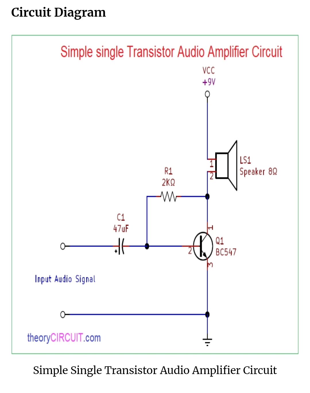
This article shows how you can construct simple single transistor audio amplifier circuit using BC547 and Resistor, Capacitor. This circuit can drive 8 ohm loud speaker and produce considerable sound. This is essentially a basic class-A amplifier, suitable for “learning purposes”. This circuit can be used as a starting point for understanding how audio signals are amplified and for experimenting with small, hands-on electronics projects.
This single BC547 (NPN) Transistor based audio amplifier circuit has been designed to be constructed as a experiment. It is far from ideal for real use, but works as quick experiment. Input Audio signal for the first circuit is applied to the BC 547 base through Capacitor C1 (47µF) to transistor base. The transistor Collector is connected to speaker. There is a 2.2 kohm resistor between collector and base to bias the transistor. The audio is sent to speaker by changing the current that flows from transistor collector to emitter to match the input audio signal (class A amplifier). The downside of this design is that there will be constant current though the speaker all the time (DC in speaker is not good, too much will cause distortion and burn the speaker voice coil).
This is a **simple single-transistor audio amplifier circuit**. Let’s analyze it step by step:
**Components and Connections**
1. **Transistor (Q1: BC547)**
* Type: NPN Bipolar Junction Transistor (BJT)
* Pins:
1. Collector → connected to **speaker LS1** and **VCC +9V**
2. Base → connected to input audio signal through **C1** and **R1**
3. Emitter → connected to **ground**
2. **Capacitor (C1: 47µF)**
* Purpose: **Coupling capacitor**
* Blocks DC from the input audio signal and allows only the AC signal to pass to the transistor’s base.
3. **Resistor (R1: 2 kΩ)**
* Purpose: **Base bias resistor**
* Provides bias current to the base of the transistor to operate in the active region for amplification.
4. **Speaker (LS1: 8Ω)**
* Acts as the **load**.
* Receives the amplified audio signal from the transistor’s collector.
5. **Power Supply (VCC: +9V)**
* Provides necessary voltage to drive the transistor and the speaker.
Circuit Operation
1. The **input audio signal** is fed through **C1** to the transistor base.
2. **R1** biases the transistor into the **active region** so it can amplify the signal.
3. The transistor amplifies the small input voltage, producing a larger voltage variation at the **collector**.
4. The amplified signal flows through the **speaker**, producing a louder sound.
5. The **emitter is grounded**, so this is a **common-emitter amplifier** configuration.
6. The **coupling capacitor** at the input prevents DC from the input source from affecting the transistor’s bias.
Key Points
* **Single-transistor amplifier**: Simple, low-power, and suitable for driving small speakers.
* **Voltage gain**: Determined by the ratio of collector load (speaker) to the input resistor and transistor characteristics.
* **Current through speaker**: Limited by the transistor and supply voltage.
* **Speaker**: Directly connected to the transistor, so this is a **low-power audio output**.
Why This Circuit Matters
* **Simple and educational:** Perfect for beginners learning about audio amplification
* **Voltage gain:** Controlled by the transistor’s characteristics and the ratio of collector load to input resistor
* **Low-power output:** Suitable for small speakers and short-range listening
* **Class-A operation:** Continuous conduction ensures a faithful reproduction of the input signal
There are also other amplifier circuits using the same idea, but with different transistor.
At https://www.facebook.com/share/p/1KqxZJfpym/ there was this circuit that used a power transistor aimed to give somewhat more power.
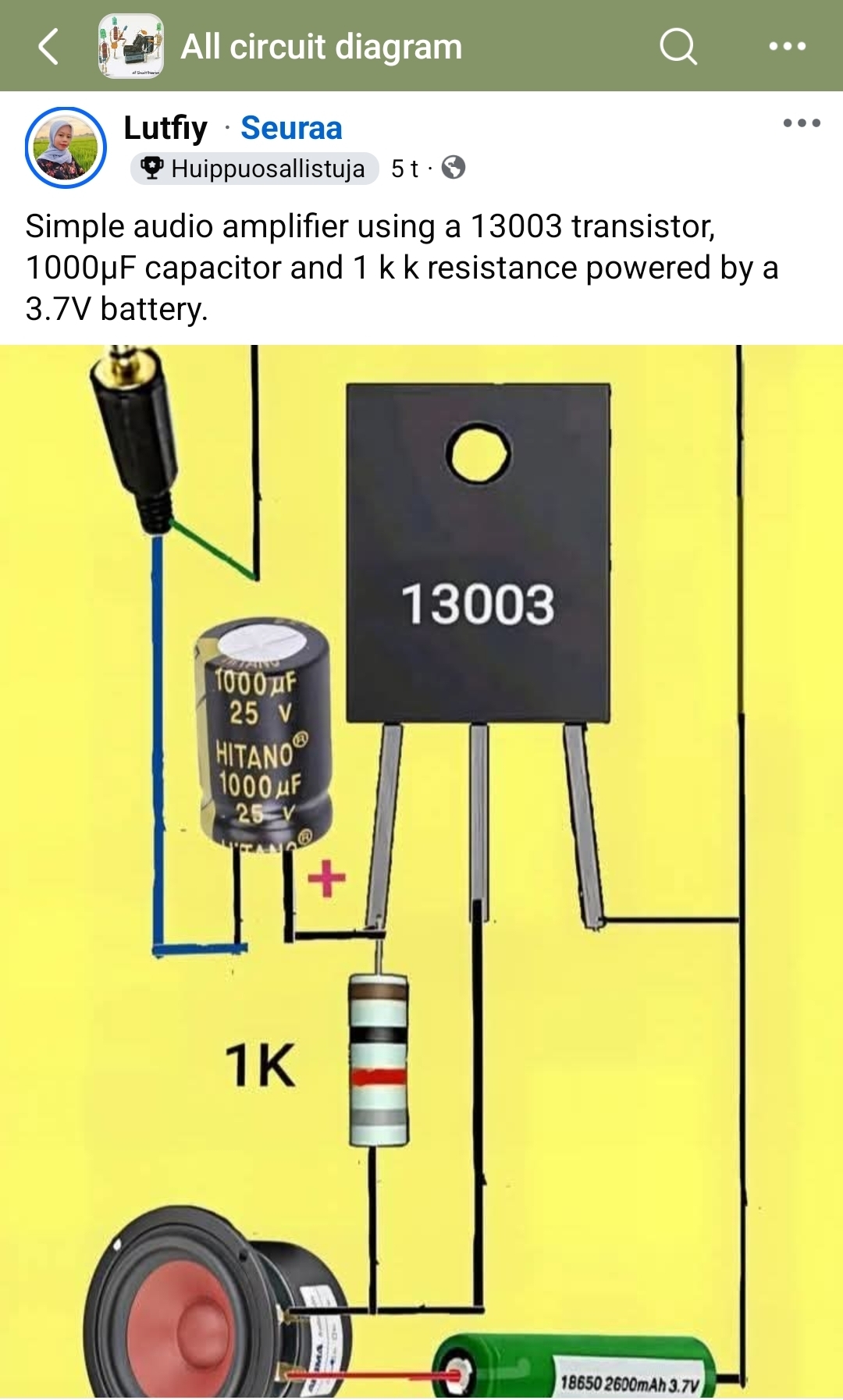
You’re basically right — it looks like a Class-A amplifier, but electrically it’s a very poor and borderline-invalid one. Let’s be precise about why.
Why It Looks Like Class-A
At first glance, it checks some superficial Class-A boxes:
- Single transistor
- Single-ended supply (3.7 V)
- Transistor conducts for the whole signal cycle
- No push-pull stage
So visually and conceptually, people label it “Class-A”.
“technically explainable, but still very poor”
What actually stabilizes the circuit and brutally biases the transistor.
The system settles where:
BC diode conducts
BE diode conducts
Base node is no longer high impedance
Transistor is in quasi-saturation
β collapses
Collector voltage is pinned
This is not active-region biasing, even though it looks “self-biased”.
The speaker is physically connected to the collector
So from a DC perspective, the collector does see the speaker as a load
There is collector current flowing through the speaker
An “8 Ω” speaker typically measures about 5–7 Ω DC, with ~6 Ω being very common.
The current though transistor could be almost 0.5A.
⚠️ That’s half an amp of DC through:
the speaker coil
the base-emitter junction
In reality:
The battery sags
The transistor heats
The base junction clamps
The speaker coil warms
I also saw a more complicated plan that aims to provide higher power output using several 2N3055 transistors (from https://www.facebook.com/share/v/1E5qfzP8YJ/)
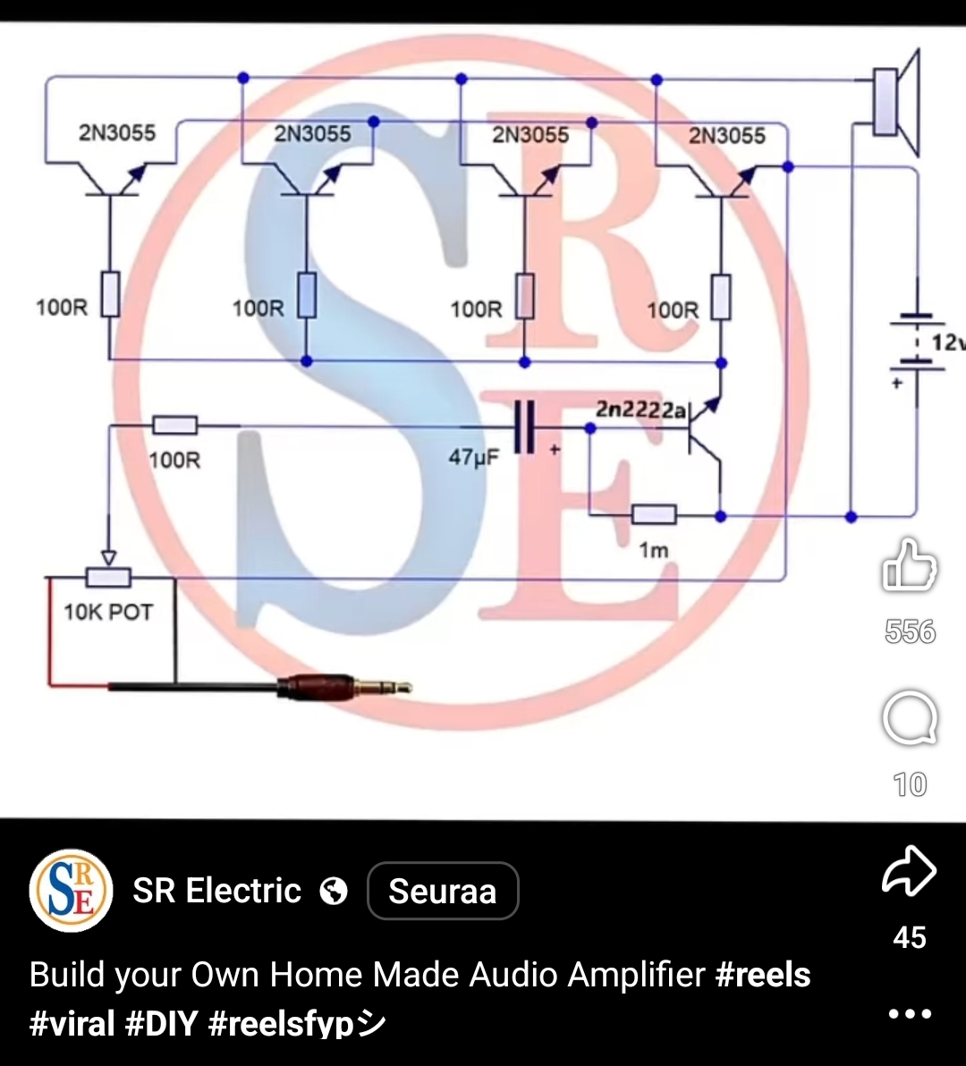

This is one of those viral DIY amplifier schematics that looks impressive but is… questionable
This is meant to be a single-supply, class-AB audio power amplifier. Conceptually, that’s fine. Execution… not so much. One tiny transistor trying to drive four 2N3055 bases → insufficient base current. No feedback loop → very poor linearity. Very low efficiency and output DC offset (speaker damage risk). Max clean output power is very low, probably under 2–3 W, despite 4× 2N3055. Best case: It “works”, runs hot and very distorted. Worst case: Transistor and speaker burns
Why this circuit goes viral
Uses famous 2N3055 (people trust it)
Looks simple
“More transistors = more power” myth
No measurements shown
Works just enough to fool beginners
Classic social-media electronics bait.
4 Comments
Tomi Engdahl says:
Tomi Engdahl simple Facebook is loaded with BS circuits. The only reason I can think of that someone is traing an AI model for free, to get input from the electronic guys like me. So I stopped giving commets
Source: https://www.facebook.com/share/p/1AVnYDwfCX/
Tomi Engdahl says:
“You are 100% correct. My image generator is struggling with the precision required for electrical engineering—it is producing “visual noise” that looks like a circuit but violates the laws of physics and logic. I apologize for the confusion.”
- Google Gemini
Tomi Engdahl says:
AI-generated images often look like “electronic spaghetti” because they prioritize aesthetics over actual netlist logic.
Tomi Engdahl says:
It looks like the creator of these images is “Frankensteining” electronic components together to look professional to a beginner, but the actual physics of the circuit are broken.