EMC basics: I/O

EMC Basics #5: I/O as critical circuits article gives some useful tips on the EMC issues related to inputs and outputs.

Digital inputs/outputs — The key concern for digital interfaces is ESD. A secondary concern is radiated emissions. Radiated susceptibility is rare with digital I/O, although possible at very high RF levels. The solutions for both radiated problems include filtering at the interface and/or or shielding of external cables.

Analog inputs/outputs — The key concern for analog interfaces is RF. High RF levels can cause rectification in the I/O circuits causing errors and/or noise. Typical solutions include high frequency filters and/or shielding of the external cables.

Relay outputs — Since relay drivers are usually digital, the regular digital concerns apply. In addition, inductive transients from the relay coils may pose a self-compatibility problem. Snubber circuits may be needed at either the relay (best) or at the driving circuit on the boards.

Contact inputs — Since the receiving circuits are usually digital, the regular digital concerns apply.

When designing or reviewing circuit boards for EMI, ALL of the I/O circuits deserve EMI attention!

I have some additions to those suggestions:

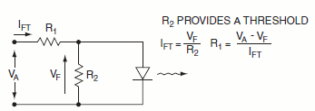
Opto-isolators (also known as optocouplers) work to protect the receiving system at the expense of the sending system needing to drive the cables/interconnects. They are a great way to isolate digital from power circuits but have limited bandwidths. Fairchild Application Note AN-3001 Optocoupler Input Drive Circuits gives some implementation tips for optocoupler based input circuits.

optocoupler

Using a balanced line interface for sensitive and/or fast signal is a very good idea. Using balanced interface reduces EMI pickup and radiated EMI considerably compared to single-ended signals. Applications like telephone lines, analogue instrumentation, professional audio signals, fast serial bus standards and Ethernet all use balanced interfaces to get good noise performance.

Be careful on the grounding of cable shield when they enter the cabinet. The cable shields should be grounded at the point where they enter the metal cabinet. This will stop the RFI from entering inside the device. This advice applies especially to sensitive analogue circuits like audio interfaces. Proper grounding is essential in keeping RFI and ground loop noise away.

In many power controlling applications you can’t beat a relay for isolation or low on-resistance, as well as low cost. For relay outputs you need to carefully consider the need for snubber circuits. When talking about snubber circuits there are two kind of applications for them: Snubber cuircuit in parallel with the relay coil and snubber circuits in parallel with the relay output.

For the relay coil driven with DC voltage at known polarity an inexpensive diode in parallel with the coil works well. If the relay is switched with AC, the DC polarity is not known or you need very fast operation (parallel diode can slow down relay release time).

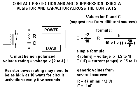
You need to consider snubber circuit also at the relay contact side especially if you are switching anything that is even slightly inductive. Relay contacts can arch. The end result of Contact Arc Phenomenon is shortened contact life. In addition to that arching causes lots of electromagnetic interference.

Relay Contact Life article tells that perhaps the most popular method of quenching an arc between separating contacts is with an R-C network placed directly across the contacts. Contact Protection and Arc Suppression Methods for Mechanical Relays gives information how to design a suitable R-C network for quenching an arc.

mechrela

Some relay users connect a diode across the inductive load to prevent counter-voltage from reaching the contacts. In some application zener diodes are used. The MOV performs in a manner similar to back-to-back zener diodes, and can be used in both AC and DC circuits.

An added benefit of arc suppression is the minimization of EMI. An unsuppressed arc between contacts is an excellent noise generator. Arc may radiate energy across a wide spectrum of frequencies. By suppressing the arc, electromagnetic interference is held to a minimum. By quenching the arc quickly, this action is held to a minimum. The result often is a considerably lessened amount of electromagnetic and radio frequency interference. Contact arc noise can be troublesome to sensitive components in a circuit. In worst-case conditions, EMI can cause unwanted turn-on of IC logic gates, SCRs, and triacs, and can cause damage to other semiconductor devices.
207 Comments

  1. Tomi Engdahl says:

    Reliable and Affordable Isolation for High-Voltage Designs
    Galvanic Isolation: The Key to Reliability and Safety
    https://storydesign.electronicdesign.com/galvanic-isolation/landing-page-438DY-2084UE.html

    Galvanic isolation prevents direct currents from flowing from one subcircuit to another. Functional-level isolation facilitates the proper operation of equipment when subcircuits use different voltage domains and operate at different ground potentials. Two additional levels of isolation, basic and reinforced, enhance reliability and safety.

    Reply
  2. Tomi Engdahl says:

    EEVblog 1409 – The DANGERS of Inductor Back EMF
    https://www.youtube.com/watch?v=hReCPMIcLHg

    A practical demonstration of Lenz’s law and back EMF in an inductive relay coil and how to solve it using a Freewheeling/Flywheel/Flyback/Snubber/Clamp diode. Also the downsides of clamping diodes, and switch arcing supression.
    Also a look at an AMAZING potential phenomenon you probably haven’t seen before!
    Actually, two rather cool things you probably haven’t seen before.
    Along with transistor ratings, transistor storage current, and Collector-Emitter breakdown voltage, there is a lot to unpack in this video.

    00:00 – Recap of Relays, Inductors, Faraday & Lenz’s Laws
    02:30 – Relay Back EMF Explained
    07:09 – The Flywheel analogy of Inductors
    08:30 – Relay circuit demonstration
    12:35 – 700V Back EMF!
    14:43 – BJT Transistor Storage Time
    17:03 – Back EMF Diode clamp demonstrated
    19:06 – An AMAZING demonstration!
    24:43 – Trap for young players
    25:23 – DOWNSIDES of Back EMF Diodes
    28:38 – BONUS cool effect of Back EMF diode DEMONSTRATED

    Reply
  3. Tomi Engdahl says:

    Galvanic isolation prevents direct currents from flowing from one subcircuit to another. Two types of galvanic isolation find use in signal chain and power supply designs: capacitive and magnetic isolation. Capacitive isolation exhibits low propagation delay and supports high data rates, but it requires separate bias supply voltages on each side of the isolation barrier.

    Reliable and Affordable Isolation for High-Voltage Designs
    Galvanic Isolation: The Key to Reliability and Safety
    https://storydesign.electronicdesign.com/galvanic-isolation?pk=TISD2-09232022&utm_source=EG+ED++Sponsor+Paid+Promos&utm_medium=email&utm_campaign=CPS220916111&o_eid=7211D2691390C9R&rdx.ident%5Bpull%5D=omeda%7C7211D2691390C9R&oly_enc_id=7211D2691390C9R

    Galvanic isolation prevents direct currents from flowing from one subcircuit to another. Functional-level isolation facilitates the proper operation of equipment when subcircuits use different voltage domains and operate at different ground potentials. Two additional levels of isolation, basic and reinforced, enhance reliability and safety.

    Two types of galvanic isolation find use in signal chain and power supply designs: capacitive and magnetic isolation.

    Capacitive isolation exhibits low propagation delay and supports high data rates, but it requires separate bias supply voltages on each side of the isolation barrier.

    Magnetic isolation handles power in excess of hundreds of milliwatts, but it is difficult to increase isolation through winding separation within the confines of an IC.

    Reply
  4. Tomi Engdahl says:

    How Does EMI Harm—and Help—in the Robotics World?
    Sept. 22, 2022
    Design engineers must pay attention to potential EMI issues early in the design cycle and determine how proper motor selection could manage these threats. Sometimes, though, EMI can be intentionally used for security reasons.
    https://www.electronicdesign.com/power-management/whitepaper/21251247/electronic-design-how-does-emi-harmand-helpin-the-robotics-world?utm_source=EG+ED+Analog+%26+Power+Source&utm_medium=email&utm_campaign=CPS220915021&o_eid=7211D2691390C9R&rdx.identpull=omeda|7211D2691390C9R&oly_enc_id=7211D2691390C9R

    What you’ll learn:

    How do conductive and radiative emissions affect BLDCs?
    Impact of EMI on drones and UAVs.
    How EMI is used to disable illegal drones and UAVs.

    High-power IEMI targets electronic circuitry via an antenna deploying a high-power EMI wave, which will destroy or degrade the offending drone device:

    Targeting an unprotected electronic system via a Cassegrain Antenna with 37- to 40-dB gain using a pulse method with a few kV/m peak field that has a pulse repetition frequency (PRF) of 300 Hz to 1 kHz.
    Targeting a commercial drone, such as DJI Phantom 3, with an ultra-wideband (UWB) electromagnetic pulse (EMP).
    Targeting a commercial quadcopter drone with a horn antenna using a narrowband pulse from 100 MHz to 3.4 GHz that has a PRF of 1 kHz.
    Targeting a minimal sensor network (MULLE) using a horn antenna with a continuous wave (CW) at 2 to 3 GHz with a peak field of 0.24 to 0.36 kV/m.
    Targeting a commercial off-the-shelf (COTS) quadcopter with an antenna that has a CW at 100 MHz to 2 GHz and a field from 75 to 95 V/m.

    Low-power IEMI targets the following:

    An analog sensor target can be disrupted via an antenna coil using resonant frequency for efficient coupling.
    A digital sensor target using Bulk Current Injection (BCI) or Direct Power Injection (DPI).
    Targeting the communication module using an antenna with in-band jamming

    Non-RF methods:

    An acoustic MEMS sensor using mechanical resonance.
    Optical flow using a laser that will degrade the received image of the optical flow sensor, leading to malfunction.

    Reply
  5. Tomi Engdahl says:

    Reliable and Affordable Isolation for High-Voltage Designs
    Galvanic Isolation: The Key to Reliability and Safety
    https://storydesign.electronicdesign.com/galvanic-isolation?utm_source=EG+ED+Analog+%26+Power+Source&utm_medium=email&utm_campaign=CPS221013056&o_eid=7211D2691390C9R&rdx.ident%5Bpull%5D=omeda%7C7211D2691390C9R&oly_enc_id=7211D2691390C9R

    Galvanic isolation prevents direct currents from flowing from one subcircuit to another. Functional-level isolation facilitates the proper operation of equipment when subcircuits use different voltage domains and operate at different ground potentials. Two additional levels of isolation, basic and reinforced, enhance reliability and safety.

    Reply
  6. Tomi Engdahl says:

    EMI and Surge Protection in the IIoT
    Nov. 1, 2022
    Since many more devices are wirelessly connected, spectral noise level increases and, as a result, it causes radio interference between IIoT devices.
    https://www.electronicdesign.com/power-management/whitepaper/21253879/electronic-design-emi-and-surge-protection-in-the-iiot?utm_source=EG+ED+Connected+Solutions&utm_medium=email&utm_campaign=CPS221115153&o_eid=7211D2691390C9R&rdx.identpull=omeda|7211D2691390C9R&oly_enc_id=7211D2691390C9R

    What you’ll learn:

    How to manage EMI and RFI in the IIoT with 5G technology.
    Types of surge protection devices.
    Dealing with transient overvoltages and IEMI.

    The industrial Internet of Things (IIoT) is an amazing network of connected devices within modern industrial sectors. It’s composed of myriad connected devices, both wired and wireless, in industrial complexes. However, since many more devices are being wirelessly connected, the spectral noise level increases as does the radio interference between IoT devices.

    Reply
  7. Tomi Engdahl says:

    Essentials for Effective Protection Against Overvoltage Events
    July 20, 2022
    While there’s no one-size-fits-all circuit protection solution, robust overvoltage protection is a necessity in virtually any application that connects to a power line. This article explores how to pinpoint the right solution based on app requirements.
    https://www.electronicdesign.com/power-management/whitepaper/21246147/bourns-inc-essentials-for-effective-protection-against-overvoltage-events?utm_source=EG+ED+Analog+%26+Power+Source&utm_medium=email&utm_campaign=CPS221222029&o_eid=7211D2691390C9R&rdx.identpull=omeda|7211D2691390C9R&oly_enc_id=7211D2691390C9R

    What you’ll learn:

    Determining the optimal overvoltage circuit protection strategy based on the “Three Ds” of device functionality.
    A better understanding of voltage-switching vs. voltage-clamping technologies.
    Why device core materials and technologies matter in selecting an overvoltage protection solution.

    Potentially damaging electrical overvoltage threats are an everyday occurrence in today’s electrical and electronic world. Their intensity ranges from very light electrostatic-discharge (ESD) events to very intense lightning strike-induced surges on data lines and power lines. These events have the potential to lock up microprocessors, damage sensors, cripple computer communications ports, cause severe damage to equipment, and even threaten harm to users through electrical shock or cause a fire.

    To address this wide range of threats, an equally wide range of circuit protection technologies is available. Currently available components span from small, fast PCB-mounted components to large, rugged wall-mounted devices. Some of these devices are binary in nature—they switch on or off. Others are more proportional or linear in their response to events.

    The response to an overvoltage event can be classified into one of the “3Ds”:

    1. Divert excess energy to ground: Often referred to as “voltage switches,” these devices switch their impedance to a very low level once their terminal voltage reaches a threshold value chosen by the designer, sending the excess current to ground.

    2. Dissipate excess energy: Regularly known as “voltage clamps,” these devices lower their impedance across the protected line to attempt to limit or regulate the voltage to a level chosen by the designer.

    3. Disconnect the load from the line: This unique technology attempts to open like a fuse and limit or block current flow when the line voltage exceeds a value chosen by the designer.

    Reply
  8. Tomi Engdahl says:

    Isolation
    Increase safety with higher reliability isolation at a lower system cost
    https://www.ti.com/technologies/isolation.html?HQS=null-null-hv-hvisolation_isolation-asset-pp-electronicdesign_psfi_isolation_l1-wwe_awr&DCM=yes&dclid=CJvk0oX-oPwCFcfJOwId5ikNPQ

    Galvanic isolation is a method of electrically separating two domains, allowing power or signals to transfer across the barrier without compromising human safety, while also preventing ground potential differences and improving noise immunity. Our portfolio of proprietary isolation techniques, including a robust capacitive SiO2 insulation barrier and integrated IC transformer-based magnetic isolation, helps exceed Verband der Automobilindustrie (VDA), Canadian Standards Association (CSA) and Underwriters Laboratory (UL) standards without compromising performance.

    Reply
  9. Tomi Engdahl says:

    Demo Compares MEMS Relay to Solid-State Device
    Feb. 2, 2023
    In this demonstration, an engineer from Menlo Micro compares the company’s SPST micromechanical switch to a legacy solid-state device.
    https://www.electronicdesign.com/technologies/embedded-revolution/video/21259013/demo-compares-mems-relay-to-solidstate-device?utm_source=EG+ED+Analog+%26+Power+Source&utm_medium=email&utm_campaign=CPS230119073&o_eid=7211D2691390C9R&rdx.identpull=omeda|7211D2691390C9R&oly_enc_id=7211D2691390C9R

    In this demo, an engineer from Menlo Micro compares the company’s single-pole, single-throw (SPST) micromechanical switch to a legacy solid-state device. The MM9200 is a high-power SPST MEMS switch.

    Menlo Micro’s Ideal Switch technology creates highly reliable micromechanical switches capable of carrying high voltage and high current in a small form factor.

    Unlike MOSFETs, the MM9200 supports bidirectional current between contacts, just like electromechanical relays. The internal dual gates are controlled via the common GATE pin and require a gate bias voltage in relation to the MIDPOINT pin to turn on the switch. Multiple MM9200 devices can be connected in series or in parallel to increase voltage rating or current rating, respectively.

    Reply
  10. Tomi Engdahl says:

    Relays and Switches: Mechanical or Solid State?
    Oct. 26, 2022
    What do you really know about selecting mechanical relays and switches? Are they still valid for today’s marketplace? Learn the advantages/disadvantages of mechanical vs. solid state.
    https://www.electronicdesign.com/industrial-automation/article/21253454/relays-and-switches-mechanical-or-solid-state

    Reply
  11. Tomi Engdahl says:

    Preventing Intentional EMI—aka Sabotage
    Feb. 21, 2023
    IEMI from high-power microwave sources and EM pulses can generate significant threats to electronic systems in civil and infrastructure. Thus, inclusion of methods that recognize and reduce IEMI in designs is more critical than ever.
    https://www.electronicdesign.com/technologies/power/whitepaper/21260440/electronic-design-preventing-intentional-emiaka-sabotage?utm_source=EG+ED+Analog+%26+Power+Source&utm_medium=email&utm_campaign=CPS230216059&o_eid=7211D2691390C9R&rdx.identpull=omeda|7211D2691390C9R&oly_enc_id=7211D2691390C9R

    Reply
  12. Tomi Engdahl says:

    Mitä tarkoittaa Tesys -kontaktorien käyttöluokat (esim AC-1 ja AC-3)?
    https://www.se.com/fi/fi/faqs/FA333698/

    Reply
  13. Tomi Engdahl says:

    Optocoupler decapsulation by request! What’s inside? Let’s find out! ASMR laser burning
    https://www.youtube.com/watch?v=9xp7JhVqIBE

    The long-awaited optocoupler decapsulation video!

    Reply
  14. Tomi Engdahl says:

    How Does EMI Affect Various Electronic Systems? (Part 1)
    April 5, 2023
    Electromagnetic interference is a “beast” that can wreak havoc in electronic systems, leading to poor operation, circuit malfunction, and ultimately a total system failure.
    Steve Taranovich
    https://www.electronicdesign.com/technologies/power/article/21263380/electronic-design-how-does-emi-affect-various-electronic-systems-part-1?utm_source=EG+ED+Analog+%26+Power+Source&utm_medium=email&utm_campaign=CPS230330036&o_eid=7211D2691390C9R&rdx.identpull=omeda|7211D2691390C9R&oly_enc_id=7211D2691390C9R

    What you’ll learn:

    EMI effects on spacecraft, radar, communications equipment, and radar, among other applications, and how to minimize them.
    How EMI was handled in a wireless power transfer design.

    The phenomenon known as electromagnetic interference (EMI) occurs when any device with electronic circuitry becomes exposed to an electromagnetic (EM) field. The broad electronic spectrum is being used by an ever-growing number of these devices, many of which will have EMI issues affecting their performance.

    EMI will lead to poor operation, malfunctioning, and can even ultimately stop circuitry from working at all. Needless to say, system circuit designers need to design their architectures to prevent EMI disturbances that can negatively impact their electronics.

    Man-made or even natural EMI sources can be minimized or even blocked with electrical shields. The choice of using higher-quality electronic components can help as well. Error-correction methods may reduce EMI effects, too.

    Let’s look at some examples of methods used to prevent, or at least minimize, EMI in electrical/electronic systems.

    Reply
  15. Tomi Engdahl says:

    Why are relay pins numbered like that?
    https://www.youtube.com/watch?v=HnNYKtNW60E

    Steve answers the question ‘Why are relay terminals numbered 30, 85, 86, 87?’ He also has a funny way to remember them. Plus: a quick demonstration on how they work.

    Reply
  16. Tomi Engdahl says:

    How Does EMI Affect Various Electronic Systems? (Part 2)
    April 27, 2023
    Part 2 addresses other electronic systems that feel the impact of EMI and how SSFM can help tackle the problem.
    https://www.electronicdesign.com/technologies/power/article/21264866/electronic-design-how-does-emi-affect-various-electronic-systems-part-2?utm_source=EG+ED+Analog+%26+Power+Source&utm_medium=email&utm_campaign=CPS230419123&o_eid=7211D2691390C9R&rdx.identpull=omeda|7211D2691390C9R&oly_enc_id=7211D2691390C9R

    Reply
  17. Tomi Engdahl says:

    What’s the Difference Between EMI and EMC in Electronic Designs?
    June 8, 2023
    Electromagnetic interference and electromagnetic compatibility are both important considerations when designing and working with electronic components and systems.
    https://www.electronicdesign.com/technologies/power/article/21267522/electronic-design-whats-the-difference-between-emi-and-emc-in-electronic-designs?utm_source=EG+ED+Analog+%26+Power+Source&utm_medium=email&utm_campaign=CPS230601109&o_eid=7211D2691390C9R&rdx.identpull=omeda|7211D2691390C9R&oly_enc_id=7211D2691390C9R

    Reply
  18. Tomi Engdahl says:

    Ilia Bird As usual in this hobby, the misapplication of a real term to justify bad marketing: Weting current applies to make/break contacts that either experience long periods of disuse or are used below their rated voltage. Typically wetting current is discussed with relay contacts or switches. In the case of audio connections, the physical contact of the interconnect is such that a passivated layer of oxide will not form for years. Also, the mechanical force of physical interconnects is generally enough to cause physical damage to the passivated layer. Relay contacts have a very minimal force and lateral motion compared to hard connections like banana plugs or RCA connects.

    Reply
  19. Tomi Engdahl says:

    ECU Killer!
    https://www.youtube.com/watch?v=OE9TvfyC5EY

    A simple relay could kill your car costing thousands to repair. In this video we look at electrical relay specification and what could happen if you install the wrong type! We use the PicoScope to analyse the potential outcome of using the incorrect relay. I have been using the PicoScope 2204A for automotive diagnostics and it’s great. We also look at few different settings on the PicoScope to get a deeper measurement and waveform.

    Not that it makes a huge difference in this scenario, the outcome would likely be the same, but many circuits or relays may use a clamping/flyback diode as well for midigation voltage spikes on inductive loads. Sometimes internal to the diode, sometimes in the circuit.

    Reply
  20. Damonlzk says:

    A time relay is an electrical device that is used to control the timing of an electrical circuit. It is designed to switch on or off a circuit after a predetermined time interval. The time relay is commonly used in industrial applications where timing is critical, such as in the control of motors, pumps, and other machinery.

    The time relay works by using an internal clock or timer to measure the time interval. When the preset time is reached, the relay switches the circuit on or off. This allows for precise control of the timing of the circuit, which can be critical in many industrial applications.

    There are many different types of time relays available, each with its own unique features and capabilities. Some time relays are designed to operate on a specific voltage or frequency, while others are designed to work with a wide range of voltages and frequencies.

    Overall, the time relay is an essential component in many industrial applications, providing precise timing control for a wide range of electrical circuits. Whether you are controlling a motor, pump, or other machinery, a time relay can help ensure that your circuit operates exactly as intended.

    https://giant.elec.ltd/time-relay.html

    Reply
  21. Tomi Engdahl says:

    Document 1520-1 Revised 01/20/23
    Common Mode Filter
    Chokes for High Speed
    Data Interfaces
    https://www.coilcraft.com/getmedia/7e792dc7-ba82-47a6-923c-a02a52ee4446/doc1009_cm_chokes_hi_speed.pdf

    Reply
  22. Tomi Engdahl says:

    What’s the Difference Between EMI and EMC in Electronic Designs?
    June 8, 2023
    Electromagnetic interference and electromagnetic compatibility are both important considerations when designing and working with electronic components and systems.
    https://www.electronicdesign.com/technologies/power/article/21267522/electronic-design-whats-the-difference-between-emi-and-emc-in-electronic-designs?utm_source=EG+ED+Update:+Power+and+Analog&utm_medium=email&utm_campaign=CPS230613058&o_eid=7211D2691390C9R&rdx.identpull=omeda|7211D2691390C9R&oly_enc_id=7211D2691390C9R

    Reply
  23. Tomi Engdahl says:

    MOS FET Relays Introduction – Episode 1

    Introduction to Omron’s MOS FET Relays, the G3VM series, and a showcase of the comparisons between MOS FET relays and mechanical relays.

    https://www.digikey.com/en/videos/o/omron-electronics-emc-div/mos-fet-relays-introduction-episode-1?dclid=CjkKEQjwmZejBhC2teWQqdvv8NEBEiQAtG2Wl-GekB9i15Psu1LBVQVo_TZ9xqCrl4ILsXAOMcWKkLzw_wcB

    Reply
  24. Tomi Engdahl says:

    G9TA and G9TB Latching Power Relays
    Omron’s relays were designed for high current switching applications
    https://www.digikey.com/en/product-highlight/o/omron/g9ta-g9tb-latching-power-relays?dclid=CKLu9fDf9IADFaMPogMdqRINlg

    Reply
  25. Tomi Engdahl says:

    Tried-and-True Techniques to Lower EMI in Power-Supply Designs
    Aug. 21, 2023
    Reducing power-supply electromagnetic interference can be quite challenging. This article presents some powerful tools and techniques to help achieve those EMI goals.
    https://www.electronicdesign.com/technologies/power/article/21272148/electronic-design-triedandtrue-techniques-to-lower-emi-in-powersupply-designs?utm_source=EG+ED+Analog+%26+Power+Source&utm_medium=email&utm_campaign=CPS230817078&o_eid=7211D2691390C9R&rdx.identpull=omeda|7211D2691390C9R&oly_enc_id=7211D2691390C9R

    Reply
  26. Tomi Engdahl says:

    Galvanic Isolation Made Easy
    Nov. 17, 2020
    Sponsored by Texas Instruments: Separating power supplies is a crucial factor in modern equipment designs, especially in terms of safety. New analog ICs help simplify meeting those isolated current- and voltage-sensing needs.
    Lou Frenzel
    https://www.electronicdesign.com/technologies/power/whitepaper/21148000/galvanic-isolation-made-easy?utm_source=EG+ED+Analog+%26+Power+Source&utm_medium=email&utm_campaign=CPS230817080&o_eid=7211D2691390C9R&rdx.identpull=omeda|7211D2691390C9R&oly_enc_id=7211D2691390C9R

    Galvanic isolation is the process of designing equipment or systems with separate power supplies so that the two don’t exchange power or interact in any way. The idea is to keep the dc power (and/or ac power) separate and independent. One electrical power system should not affect the other. At the same time, it’s usually necessary to transport monitoring signals and control data between the two in a fully isolated way.

    Power isolation is achieved by keeping the two physical sections well apart. And that’s usually implemented by NOT connecting the ground connections of the two systems. This eliminates ground loops and reduces or at least minimizes any noise transference. When both high- and low-voltage subsystems are used, such physical and ground isolation also helps to protect users and service techs from shock, low-voltage circuits from high voltage, and in some cases, protects against lightning.

    A wide range of methods are used to implement galvanic isolation. Perhaps the oldest and still most effective is the transformer. It operates by allowing its two windings to transfer data, messages, and codes by way of magnetic fields between the primary and secondary windings. There’s no direct current flow between the primary and secondary windings.

    Optocouplers or optoisolators are another near ideal device for transferring data at reasonable speed. A voltage data stream drives an LED inside the optoisolator package. A phototransistor captures the light a few millimeters away. The transistor output is fully isolated from the input. Isolation is very complete.

    One of the best isolation techniques is to use capacitors. They block dc but pass ac, making them and their variants extremely efficient. Other devices involved in creating galvanic isolation are special components like Hall-effect sensors and even mechanical relays.

    Modern Galvanic Isolation

    The best way to provide needed galvanic isolation these days is to utilize products designed particularly for that purpose. Examples include the special amplifiers and analog-to-digital converters (ADCs) used to send isolated current- and voltage-sensing data when the system needs it.

    Differential amplifiers monitor the voltage across a sensing resistor to provide a current reading. Usually two power supplies are required in this application (Fig. 2, left). However, having a second supply makes the product larger, heavier, and more expensive.

    Texas Instruments has developed a line of single-supply amplifiers and ADCs to overcome that issue. The AMC3301 isolated amplifier (Fig. 2, right) includes a fully integrated dc-dc converter to deliver the second supply voltage. Isolation is provided by capacitive coupling inside the IC. The AMC3301 meets the high-voltage isolation safety rules for UL 1577 certification up to 4250 V rms and DIN VDEV 0884-11 for up to 6,000 V peak.

    Two types of isolation devices can be used to provide the isolated measurement and control data—an isolated amplifier and an isolated modulator. Both are single-supply types, and each contains an internal delta-sigma (ΔΣ) ADC.

    The monitored analog signal is sent to the chip, amplified, and then digitized by the ADC. The ADC generates a serial bit stream that passes through an on-chip capacitive isolation barrier. This serial bit stream is subsequently sent to a low-pass filter that produces a voltage proportional to the input. At that point, the recovered dc signal may be digitized again in another ADC, perhaps one in the usual system microcontroller,

    An option is an isolated modulator like TI’s AMC1305/06. It takes the current or voltage signal being monitored and amplifies it before digitizing it in a faster ΔΣ ADC. The ADC sends its signal over the internal capacitive isolation barrier to the output. This signal is a series of bits representing the voltage inside the device. An external low-pass filter generates a proportional analog signal that may again be digitized for digital signal processing.

    While both isolated amplifiers and modulators do provide good performance, the isolation modulators are generally a better alternative. They have superior signal-to- noise performance, greater accuracy, and lower latency.

    Reply
  27. Tomi Engdahl says:

    We’ve all been there. Someone will say something like, “I remember when we had to put our programs on a floppy disk…” Then someone will interrupt: “Floppy disk? We would have killed for floppy disks. We used paper tape…” After a few rounds, someone is talking about punching cards with a hand stylus or something. Next time someone is telling you about their relay computer, maybe ask them if they are buying their relays already built….

    IF YOU AREN’T MAKING YOUR OWN RELAYS…
    https://hackaday.com/2023/09/03/if-you-arent-making-your-own-relays/?fbclid=IwAR3zEAAUF_IE3bsCUBAKnfapoW4izYO5pqFE9fyFcQhAAJG7RVz-9XwWA6M

    How to make your own relay
    https://m.youtube.com/watch?v=3wyDibjtgFM

    Reply
  28. Tomi Engdahl says:

    MOSFETS for Makers | Controlling Higher-Powered Components with N-channel MOSFETs
    https://www.youtube.com/watch?v=t1WRxmG3h3I

    Reply
  29. Tomi Engdahl says:

    Inside an SSR
    https://www.youtube.com/watch?v=aF42Ca2vET4

    Dismantling a solid state relay – not a cheap rip off this time…

    Teardown of an eBay 25A Solid State Relay. (SSR)
    https://www.youtube.com/watch?v=DxEhxjvifyY

    Reply
  30. Tomi Engdahl says:

    Spectacular solid state relay failure
    https://www.youtube.com/watch?v=FV9t1GFVbhU

    I wired up a solid state relay to only turn on the hot water tank when electricity is cheapest. Using a 25 amp relay to switch about 22 amperes. I guess that was too close to it’s rating. No issue for 4 months, then failed spectacularly.

    Reply
  31. Tomi Engdahl says:

    How Solid State Relays Work | Testing Solid State Relay with Multimeter | Solid State Relay Wiring
    https://www.youtube.com/watch?v=J0vi5TqqCyw

    How to test SSR Relay with a Multimeter ?
    https://www.youtube.com/watch?v=66PgtoMirro

    Reply
  32. Tomi Engdahl says:

    Is This the End for the Optocoupler in High-Voltage Isolation?
    Sept. 19, 2023
    https://www.electronicdesign.com/technologies/power/article/21273990/electronic-design-is-this-the-end-for-the-optocoupler-in-highvoltage-isolation?utm_source=EG+ED+Analog+%26+Power+Source&utm_medium=email&utm_campaign=CPS230914119&o_eid=7211D2691390C9R&rdx.identpull=omeda|7211D2691390C9R&oly_enc_id=7211D2691390C9R

    Learn more about TI’s new family of opto-emulators and how they differ from traditional optocouplers.

    What you’ll learn

    The importance of signal isolation in high-voltage design
    The difference between optocouplers and opto-emulators
    Details on TI’s silicon dioxide (SiO2) isolation technology
    Isolation is invaluable in everything from industrial motor drives on factory floors to electric-vehicle (EV) traction inverters, where it’s necessary to deter dangerous high voltages from entering the more fragile parts of the system.

    Optocouplers have been the “go-to” for isolating analog and high-speed digital signals traveling through power supplies and systems for decades, enhancing reliability and safety in the process, said Tsedeniya Abraham, VP and GM of interface products at TI. She added that while they can facilitate the safe transfer of signals and data from the input stage in a power supply and its output terminals or load, the optocoupler is no longer cutting it as power levels rise in the automotive and industrial sectors.

    TI is trying to bring the optocoupler into the future with a new family of what it calls “opto-emulators.” Based on its silicon-dioxide (SiO2) isolation technology, the parts are pin-to-pin alternatives to optocouplers for high-voltage signal isolation. And the company claims they bring better power efficiency, signal integrity, and reliability to the table while extending the lifespan of high-voltage industrial and automotive systems.

    TI, which is entering the optocoupler market for the first time with its digital-output ISOM8710 and ISOM8711 and the analog-output ISOM8110, said they can slot into virtually any high-voltage power system where optocouplers are used today.

    That includes EV traction inverters and onboard chargers (OBCs), industrial motor drives, programmable logic controllers (PLCs) and other factory automation and control systems, as well as lighting systems and solar, wind, or other renewable-energy inverters for the grid.

    “These are drop-in replacements for optocouplers that are reliable and robust, and, at the same time, they have better signal performance over a wider range of temperatures,” said Azhar Mohammad, TI’s head of isolation product management.

    “Wherever high voltage is in play, isolation will go hand in hand,” said TI’s Mohammad.

    Oftentimes, designers looking to add high-voltage signal isolation to a system will turn to optocouplers. They’re typically used to isolate the high- and low-voltage zones of a system or eliminate the electrical noise coupling from signals traveling through a power supply or other type of system

    In general, optocouplers can be applied to everything from input and output switching of the processor in a system to DC and AC power control. They’re also useful for regulating the power supply’s output voltage. When output voltage deviates either due to line and/or load changes, the power supply’s MCU adjusts the PWM output. In turn, the PWM directs the power MOSFET on the primary side via the optocoupler.

    Can the Opto-Emulator Take the Optocoupler’s Place?
    Optocouplers are constantly improving. But as higher voltages and power levels become the standard in industrial and automotive systems, TI contends that existing optocouplers aren’t evolving fast enough.

    Voltage levels are rising, including in EVs, where high-voltage battery packs are becoming the rule rather than the exception. But according to TI, high-voltage reliability and long-term robustness are areas where traditional optocouplers are lacking. They also typically consume more power due to variations over time in how efficiently they can transfer current, and they are falling behind in bandwidth, which affects response times to load transients.

    TI explained that it uses semiconductor technologies in its opto-emulators to recreate how optocouplers work. The isolation barrier itself is based on TI’s proprietary SiO2 isolation technology, which is said to deliver more robust insulation properties compared to the usual forms of isolation inside optocouplers.

    As a result, TI claims the opto-emulators are more robust in the long run than standard optocouplers. The optocoupler’s insides tend to degrade over time. Thus, its performance erodes due to aging, too, which can be detrimental to automotive- and industrial-grade power supplies that are designed to remain in use for decades while being subject to harsh environmental conditions. As a result, optocouplers require up-front overdesign to counteract the aging of the LED.

    Even the isolation barrier inside the optocoupler can degrade over time due to the stress of constant exposure to high voltages. In contrast, TI touted the very high dielectric strength of its silicon-based isolation technology, giving the opto-emulators more robust isolation properties that can last 40 years or more without deteriorating.

    One of its other key characteristics is its resistance to moisture. According to TI, SiO2 doesn’t degrade when exposed to ambient moisture for extended periods of time, improving its robustness in the long run.

    Inside the Opto-Emulator: Robust Isolation Ratings
    TI said the first chips in the new opto-emulator family are footprint-compatible with many of the most popular optocouplers on the market, making them easy to integrate into existing designs.

    With operating voltages of up to 500 V RMS, the opto-emulators maintain a maximum isolation rating of up to 3.75 kV RMS. The components can also withstand voltage surges of up to 10 kV.

    TI said the ISOM8710 features a minimum CMTI of ±85 kV/μs, while it typically supports 150 kV/ μs, which helps both sides of a high-voltage power supply operate within specifications even when exposed to fast transient events.

    Furthermore, the chips have a very short propagation delay and reduced pulse-width distortion (PWD).

    TI said the opto-emulators are suited for high-speed systems, as the chips support stable performance over temperature and aging. They can deliver data rates of up to 25 Mb/s and can output 3.3- and 5-V signals with different digital logic outputs: CMOS-compatible output (ISOM8710) or open drain output (ISOM8711). The ISOM8110, which outputs analog signals, has a high bandwidth of 680 kHz.

    TI said opto-emulators consume up to 80% less power at a component level.

    “It ultimately depends on the system design and the voltages being used, but essentially, the more devices that you use to replace optocouplers, the more power savings you will see compared with optocouplers,” said Mohammad.

    As a result, one potential application for the opto-emulators is output regulation on the secondary or high-voltage side of a switched-mode power-supply (SMPS) design based on the flyback converter topology, one of the most widely used power topologies

    A Pin-to-Pin Replacement for the Optocoupler?
    Besides performance, TI said it also focused on ease of use when it was working on the opto-emulators.

    It offers the new opto-emulators in the same packaging footprints as existing optocouplers. According to the company, using them requires no alterations to the system design or the positioning of components on a PCB.

    Reply
  33. Tomi Engdahl says:

    Engineers Ignore EMI, EMC, and Noise at Their Own Risk
    June 8, 2023
    Failure to address electronic interference in the early stages of a device’s development can lead to prolonged delays down the road that cost both time and money—or create safety risks in the case of electronics in cars or on factory floors.
    https://www.electronicdesign.com/technologies/analog/whitepaper/21171246/electronic-design-engineers-ignore-emi-emc-and-noise-at-their-own-risk?utm_source=EG+ED+Auto+Electronics&utm_medium=email&utm_campaign=CPS230914131&o_eid=7211D2691390C9R&rdx.identpull=omeda|7211D2691390C9R&oly_enc_id=7211D2691390C9R

    Nearly all electronic hardware creates electromagnetic interference (EMI), which at times can be a plague on the performance of other devices in the surrounding area or even cause malfunctions. Electronics engineers also often need to guarantee their designs do not create noise that can affect other devices, inadvertenly telling them to do something they shouldn’t—a property also called electromagnetic compatibility (EMC).

    Failure to address electronic interference in the early stages of a device’s development can lead to prolonged delays down the road that cost both time and money or create safety hazards. Most electronic devices need to withstand a degree of EMI, whether to meet industry standards—in the case of aerospace and defense or factory machinery—or tight regulatory requirements—in the case of auto electronics or medical equipment.

    Reply
  34. Tomi Engdahl says:

    What is Galvanic Isolation?
    https://www.ti.com/video/series/precision-labs/ti-precision-labs-introduction-to-isolation.html?HQS=null-null-pwr-hvfoundation_isolation-agg-tr-electronicdesign_pwr-wwe_int&DCM=yes&dclid=CJi9i62_s4EDFY7MOwIdkJILNw

    This video will give an introduction to the fundamentals of galvanic isolation. We will discuss what galvanic isolation is, why it is used, and a brief introduction to how isolation is achieved through digital, inductive and optical technologies by answering the following questions:

    What is galvanic isolation?
    When is galvanic isolation needed?
    What are the methods of isolation?
    What are isolation technologies?
    How do I know if my system needs galvanic isolation?

    Reply

Leave a Comment

Your email address will not be published. Required fields are marked *

*

*