Nowadays you can find many low-cost microcontroller devboards (starting from just few dollars/euros). More recently, we’ve seen ARM Cortex kits for $10-$50, the flowering of the whole Arduino ecosystem, and of course, the Raspberry Pi. It’s microcontroller heaven with very many dev boards available. You you want more performance, there is a wide selection of Linux friendly single board computers in around $35 to $200 range.
What do you want to try next after microcontroller dev boards? Maybe FPGA. A field-programmable gate array (FPGA) is an integrated circuit designed to be configured by a customer or a designer after manufacturing. FPGAs contain programmable logic components called “logic blocks”, and a hierarchy of reconfigurable interconnects that allow the blocks to be “wired together” – somewhat like many (changeable) logic gates that can be inter-wired in (many) different configurations. Logic blocks can be configured to perform complex combinational functions, or merely simple logic gates like AND and XOR.
Those of us wanting a cheap “in” to the FPGA world have been less lucky than developers looking for microcontroller dev boards. FPGA boards under $100: Introduction article is indicting that the times, they are a changin’. Many FPGA devkits, from both chipmakers and third parties, have broken – or downright shattered – the $100 barrier, opening the door to low-cost FPGA prototyping, education, hobby projects, and so on. FPGA boards under $100: Introduction article offers a good overview of what is available.
Here are some interesting additions to the listed boards:
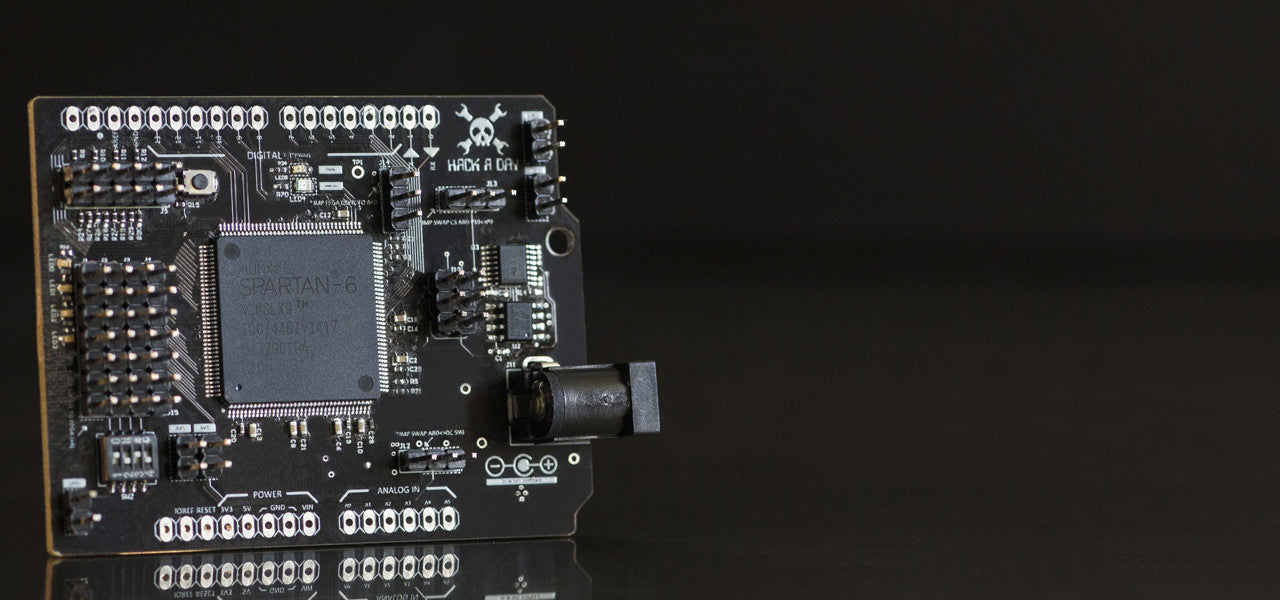
Hacklet 28 – Programmable Logic Hacks posting tells about Arduino-Compatible FPGA Shield. The shield features a Xilinx Spartan 6 FPGA and is available in The Hackaday Store. It has the needed regulators and level shifters. The price is $69.97. Not sure where to start? Check out Spartan-6 FPGA Hello World! that uses Xilinx’s free tool chain to getting a “hello world” led blinker running!
Hacklet 28 – Programmable Logic Hacks posting also mentions Chameleon. Chameleon is an Arduino compatible FPGA board with a Xilinx Spartan 3A FPGA on-board. The Chameleon Arduino-compatible shield board was designed to support two general application areas: (1) soft-core processors, and (2) intelligent serial communications interface.
Cheap FPGA-based HDMI Experimenting Board project is designing a (relatively) cheap little board for experimenting with HDMI using a Spartan-6 FPGA.
432 Comments
Tomi Engdahl says:
Data Centers Dominate FPGA Event
http://www.eetimes.com/author.asp?section_id=36&doc_id=1330431&
In a sign of the times, four out of the five keynote presentations at FPL 2016, a major FPGA conference in Europe, were given by large companies such as IBM, Intel and Microsoft focused on the efficient deployment and use of FPGAs in data centers.
Christoph Hagleitne presented IBM’s view of the major applications where FPGAs can provide differentiation such as cognitive computing, high performance computing and the Internet of Things. He described two complementary approaches to establish heterogeneous computing systems in cloud datacenters.
The first approach is based on heterogeneous supernodes that tightly couple compute resources to multi-core CPUs and their coherent memory system via high-bandwidth, low latency interconnects like CAPI or NVlink. The second approach is based on the disaggregation of data center resources where the individual compute, memory, and storage resources are connected via the network fabric and can be individually optimized and scaled in line with the cloud paradigm.
Hagleitne described IBM’s SupperVessel platform, a cloud service created by IBM Research in Beijing and IBM Systems Labs that is part of the OpenPower initiative. SupperVessel is based on Power processors, with FPGAs and GPUs providing acceleration services, using OpenStack to manage the whole cloud. He also presented the new interfaces IBM’s Power 9 processor will use for fast communication between the processor and the accelerators.
P. K. Gupta, the general manager of Xeon+FPGA products in Intel’s data center group, said FPGAs can increase the performance of applications such as machine learning, cloud radio-access networks, edge computing and content delivery. Accelerators can increase performance at lower total cost of ownership for targeted workloads, he said.
FPGAs can be deployed in data centers both in discrete platforms and in integrated platforms in multi-chip packages, Gupta said.
Finally, Xilinx presented a new open-source framework called Pynq for designing with its Zynq FPGAs. Pynq enables programmers who design embedded systems to exploit the capabilities of SoCs based on Zynq chips without having to use CAD tools to design programmable logic circuits. Instead the SoCs are programmed in Python and the code is developed and tested directly on the embedded system. The programmable logic circuits are imported as hardware libraries and programmed through their APIs, essentially the same way that software libraries are imported and programmed.
Tomi Engdahl says:
How High-Level Synthesis Was Used To Develop An Image-Processing IP Design From C++ Source Code
http://semiengineering.com/how-high-level-synthesis-was-used-to-develop-an-image-processing-ip-design-from-c-source-code/
Methodology helped accommodate late spec changes on aggressive delivery schedule.
Imagine working long and hard on a design, only to learn that you need to add new (and more complex) functionality a few months before your targeted tapeout. How can you deliver the performance and capabilities expected in the same timeframe? For Bosch, high-level synthesis (HLS) provided the solution. In this paper, we will discuss how HLS technology enabled the team to meet an aggressive schedule on its image-processing IP without any changes to its existing floorplan.
https://www.cadence.com/content/dam/cadence-www/global/en_US/documents/tools/digital-design-signoff/bosch-high-level-synthesis-wp.pdf
Tomi Engdahl says:
Hackaday Prize Entry: FPGAs For The Raspberry Pi Zero
http://hackaday.com/2016/10/02/hackaday-prize-entry-fpgas-for-the-raspberry-pi-zero/
The Raspberry Pi is the Arduino of 2016, and that means shields, hats, add-ons, and other fun toys that can be plugged right into the GPIO pins of a Pi. For this year’s Hackaday Prize, [Valentin] is combining the Pi with the next age of homebrew computation. He’s developed the Flea Ohm, an FPGA backpack or hat for the Pi Zero.
The Flea Ohm is based on Lattice’s ECP5 FPGA featuring 24k LUTs and 112kB BRAM. That’s enough for some relatively interesting applications, but the real fun comes from the added 32MB or 128MB of SDRAM, a micro SD card slot, USB + PS/2 host port and an LVDS output.
‘Flea Ohm’ FPGA Project
https://hackaday.io/project/13048-flea-ohm-fpga-project
My own raspi-zero style board, based on the new ECP5 series FPGA from Lattice Semiconductor!
Tomi Engdahl says:
Demo board packs 50-Msample/s DAC
http://www.edn.com/electronics-products/other/4442768/Demo-board-packs-50-Msample-s-DAC?_mc=NL_EDN_EDT_EDN_today_20161003&cid=NL_EDN_EDT_EDN_today_20161003&elqTrackId=4382610133214281a64e8c66851bd3f5&elq=96414a4287c645e48fa863997e40669d&elqaid=34144&elqat=1&elqCampaignId=29825
Leveraging the company’s LTC1668 50-Msample/s, 16-bit DAC, the DC2459A demonstration circuit from Linear Technology accepts digital signals from one of several FPGA development boards. Example FPGA code is also provided, which produces digital sine-wave data for the DAC. At an output signal frequency of 1 MHz, the converter achieves high spectral purity, exhibiting a spurious free dynamic range of 87 dB.
One of the digital connectors on the DC2459A board is directly compatible with the Mojo Spartan 6 FPGA board from Embedded Micro.
Other FPGA boards that work with the DC2459A demo circuit include the Numato Labs Mimas and Altera DE0-Nano, as well as 3.3-V HSMC (high-speed mezzanine card) FPGA boards.
DC2459A-A – LTC1668 with LT1812 Demo Board | 16-Bit, 50Msps DAC, Single-Ended ±1V outputs
http://www.linear.com/solutions/7220
Tomi Engdahl says:
Open Design Oscilloscope Could be (Almost) Free
http://hackaday.com/2016/10/06/open-design-oscilloscope-could-be-almost-free/
If you could only own one piece of test equipment, it should probably be an oscilloscope. Then again, modern scopes often have multiple functions, so maybe that’s not a fair assertion. A case in point is the Scopefun open hardware project. The device is a capable 2-channel scope, a logic analyzer and also a waveform and pattern generator. The control GUI can work with Windows, Linux, or the Mac
The hardware uses a Xilinx Spartan-6 FPGA. A GUI uses a Cypress’s EZ-USB FX2LP chip to send configuration data to the FPGA. Both oscilloscope channels are protected for overvoltage up to +/- 50 V. The FPGA samples at 100 Mhz through a 10-bit dual analog-to-digital converter ( ADC ). The FPGA handles triggering and buffers the input before sending the data to the host computer via the USB chip. Each channel has a 10,000 sample buffer.
A 16-bit digital interface can be set as inputs or outputs. The FPGA samples inputs at 100 MHz.
ScopeFun – Open Source Oscilloscope
http://www.scopefun.com/
Specifications
100 Mhz Real-Time Sampling rate / 3.2 Ghz Equivalent-Time Sampling rate
2 analog oscilloscope channels (10-bit)
2 analog generators (12-bit)
16 digital channels (logic analyzer / pattern generator)
USB 2.0 interface
Tomi Engdahl says:
Xilinx bolsters low-end & midrange offerings
http://www.edn.com/electronics-products/other/4442780/Xilinx-bolsters-low-end—midrange-offerings?_mc=NL_EDN_EDT_EDN_today_20161010&cid=NL_EDN_EDT_EDN_today_20161010&elqTrackId=40199c9bc9884558b86897658e14ff37&elq=db66a391d2644c798950cb756a5e6d9a&elqaid=34281&elqat=1&elqCampaignId=29917
Aiming at applications including embedded vision and industrial IoT, Xilinx has added parts in what it terms its cost-optimized offering, across its Spartan, Artix, and Zynq families, for any-to-any connectivity, sensor fusion, precision control, image processing, analytics, safety, and security.
Return of the Spartans
The company says that this portfolio expansion, “…now including the Spartan-7 family, additional Artix-7 products, and Zynq-7000 single core devices, offers the most compelling performance-per-watt solutions in the industry and expanded processor scalability all at lower cost entry points.”
The Spartan-7 family is positioned as the only 28nm-based FPGA in an 8 × 8 mm package, enabling the portfolio’s most cost-efficient connectivity solution for both legacy and cutting-edge interfaces, while delivering the highest performance-per-watt sensor fusion and precision control in a small form factor. The new Spartans use half the power yet provide 30% more performance compared to the previous generation, and come in 6 – 102 kLE sizes with up to 400 I/Os.
Tomi Engdahl says:
An Open Source 96 MSPS Logic Analyzer For $22
http://hackaday.com/2016/10/26/an-open-source-96-msps-logic-analyzer-for-22/
If you are in the market for an inexpensive USB logic analyser you have a several choices, but few of them deliver much in the way of performance. There are kits from China for a few dollars using microcontrollers at their heart, but they fail to deliver significant sample rates. If you require more, you will have to pay for it.
It is therefore rather interesting to see [kevinhub88]’s SUMP2 project, an open source logic analyser with a claimed 96 MSPS sample rate using an off-the-shelf Lattice iCEstick FPGA evaluation board that only costs about $20. It talks to a host computer via USB using the established SUMP protocol, so its software front-end comes from the sump.org logic analyser project.
$22 FPGA-Based Logic Analyzer Packs a Punch
http://www.eetimes.com/author.asp?section_id=216&doc_id=1330689&
The FPGA-based SUMP2 logic analyzer is useful for large FPGA development, but is also able to scale way down to work on a $22 Lattice iCEstick FPGA+USB board.
Kevin’s latest project is the open source SUMP2 Logic Analyzer — an FPGA-based tool that is useful for large FPGA development, but that is also able to scale way down to work on a $22 Lattice iCEstick FPGA+USB board.
The SUMP2 Logic Analyzer offers 96 MSPS at 16-bits LVCMOS with real-time hardware compression, and the SUMP2 section on the Black Mesa Labs website provides everything you need to get you up and running (apart from the $22 Lattice iCEstick).
So, a big thanks to Kevin for making the SUMP2 available to the community.
SUMP2 – 96 MSPS Logic Analyzer for $22
https://blackmesalabs.wordpress.com/2016/10/24/sump2-96-msps-logic-analyzer-for-22/
Tomi Engdahl says:
Embedded FPGAs Going Mainstream?
http://semiengineering.com/will-efpgas-go-mainstream/
Programmable devices are being adopted in more market segments, but they still haven’t been included in major SoCs. That could change.
Systems on chip have been made with many processing variants ranging from general-purpose CPUs to DSPs, GPUs, and custom processors that are highly optimized for certain tasks. When none of these options provide the necessary performance or consumes too much power, custom hardware takes over. But there is one type of processing element that has rarely been used in a major SoC— the FPGA.
Solutions implemented in FPGAs are often faster than any of the instruction-set processors, and in most cases they complete a computation with lower total energy consumption. However, their overall power consumption is higher, and performance is slower than custom hardware. In addition, they use a lot more silicon area because the FPGA is a fixed resource, so enough of it must be put onto a chip for what is believed to be the worst-case usage scenario.
The standalone FPGA market currently is dominated by two companies, Xilinx and Altera (Intel). Part of the reason for this is they do not just produce chips. FPGAs require a complex ecosystem to make them useable. This ecosystem is very similar to those required for supporting processors. The transformation from FPGA to eFPGA adds even more complexity to this ecosystem because it requires a customized toolchain for each IP core that is licensed.
Tomi Engdahl says:
The Battle To Embed The FPGA
http://semiengineering.com/the-battle-to-embed-the-fpga/
It has always seemed like a good idea but nobody has managed to pull it off so far. Will one of the recent contenders be successful?
There have been many attempts to embed an FPGA into chips in the past, but the market has failed to materialize—or the solutions have failed to inspire. An early example was Triscend Corporation, founded in 1997 and acquired by Xilinx in 2004. It integrated a CPU—which varied from an ARM core to an 8051—memory and the programmable fabric into a microcontroller.
Another example was Stretch, which attempted to build extensions for Tensilica products.
“There is an impedance mismatch – you optimize architectures differently in an FPGA and an ASIC,” says Drew Wingard, chief technology officer at Sonics. “FPGAs tend to be frequency challenged, so you tend to go wider and slower and exploit parallelism. Typically, it means that it is difficult to tightly couple an FPGA in the execution path of a CPU.”
Geoffrey Tate, CEO of Flex Logix, adds a larger list of failed products: “Actel, IBM, Leopard Logix, LSI Logic, Tabula, Velogix, and probably more.”
Perhaps the most viable reason for the adoption of FPGAs in the past was when you were developing an ASIC that implemented a standard that wasn’t quite finished. Everyone was anxious to get the product out, but the spec was not yet finalized. So you could put part of it into an FPGA, and as the spec continued to evolve you could update the logic appropriately. This was then designed out in the next generation of the product to reduce cost.
Another reason was for bug fixing.
To date, solutions that deploy an external FPGA have been more successful than those that attempted to integrate it.
“In the early ’80s the chips were fairly small, low in performance, and used as TTL glue logic integration. They replaced multiple logic parts on the board. That brought the market to around $500M. In the next phase, FPGAs grew with Moore’s Law and got to be bigger, faster and cheaper. As the complexity grew, the main application that took them to $5B was associated with connectivity. I/O standards did not always connect well, so FPGAs were used to bridge the connectivity. FPGAs were used broadly in networking infrastructure equipment.”
Blake sees that we are entering a new phase. “They will start to get used as a co-processor. FPGAs are very good at building arbitrary width datapath engines. This means they can be used for datacenter exploration, adding significant flexibility to software-defined networks. And as 5G infrastructure rolls out, the FPGAs will be used heavily for the digital front end and for customization of different marketplaces.”
40nm and 28nm have large amounts of logic available making the overhead of the FPGA less of an issue.
Tomi Engdahl says:
Give Your RPi a Cool FPGA Hat
http://hackaday.com/2016/11/05/give-your-rpi-a-cool-fpga-hat/
Need additional, custom IO for your Raspberry Pi? Adding an FPGA is a logical way to expand your IO, and allow for high speed digital interfaces. [Eric Brombaugh]’s Icehat adds a Lattice iCE5LP4K-SG48 FPGA in a package that fits neatly on top of the Raspberry Pi Zero. It also provides a few LEDs and Digilent compatible PMOD connectors for adding peripherals. The FPGA costs about six bucks, so this is one cheap FPGA board.
icehat – Raspberry Pi ice40 Ultra FPGA hat
http://ebrombaugh.studionebula.com/embedded/icehat/index.html
Tomi Engdahl says:
New Part Day: Pynq Zynq
http://hackaday.com/2016/11/04/new-part-day-pynq-zynq/
FPGAs are the future, and there’s a chip out there that brings us the future today. I speak, of course, of the Xilinx Zynq, a combination of a high-power ARM A9 processor and a very capable FPGA. Now the Zynq has been made Pynq with a new dev board from Digilent.
The heart of this board, is, of course, the Xilinx Zynq packing a Dual-core ARM Cortex A9 processor and an FPGA with 1.3 Million reconfigurable gates. This is a dev board, though, and with that comes memory and peripherals. To the board, Digilent added 512MB of DDR3 RAM, a microSD slot, HDMI in and out, Ethernet, USB host, and GPIOs, some of which match the standard Arduino configuration.
PYNQ-Z1 board
http://www.pynq.io/board.html
The PYNQ-Z1 board is the first Zynq board to oficially support PYNQ. The board features a Zynq XC7Z020, Ethernet, HDMI in/out, MIC in, Audio out, Arduino Interface, 2 Pmods, 16 pin GPIO header, user LEDs, pushbuttons and Switches.
Compatible Arduino shields and Pmod accessories can be used with the board. The interfaces can also be used as GPIO.
The PYNQ Shield is compatible with the Arduino interface, and provides 16 Grove sockets (4 Analog, 4 I2C, 1 UART and 7 GPIO). The PYNQ shield also has a pass-through header for the Arduino pins, and the 16 pin GPIO header on the PYNQ-Z1 board.
The PYNQ Grove Adapter has four Grove sockets and can be connected to a Pmod port allowing up to four Grove devices to be used with a single Pmod.
Tomi Engdahl says:
An Open Source Toolchain For iCE40 FPGAs
http://hackaday.com/2015/05/29/an-open-source-toolchain-for-ice40-fpgas/
FPGAs are great, but open source they are not. All the players in FPGA land have their own proprietary tools for creating bitstream files, and synthesizing the HDL of your choice for any FPGA usually means agreeing to terms and conditions that nobody reads.
After months of work, and based on the previous work of [Clifford Wolf] and [Mathias Lasser], [Cotton Seed] has released a fully open source Verilog to bitstream development tool chain for the Lattice iCE40LP with support for more devices in the works.
https://github.com/cseed/arachne-pnr
Tomi Engdahl says:
Microsemi Offers First FPGA-Based RISC-V IP Core
http://www.eetimes.com/document.asp?doc_id=1330851&
Microsemi (Aliso Viejo, Calif.) has just become the first FPGA provider to offer the open architecture RISC-V as a soft IP processor core, along with a comprehensive software tool chain for embedded designs.
Pronounced “Risk Five,” the RISC-V is not a processor core per se; instead, it is an open-source instruction set architecture (ISA) that is based on established reduced instruction set computing principles.
The RISC-V ISA was designed from the ground-up to be useful in modern computerized devices, ranging from warehouse-scale cloud computers to high-end smartphones to the smallest embedded systems.
In contrast to most ISAs, RISC-V is freely available for all types of use, permitting anyone to design, manufacture, and sell RISC-V chips and software. The fact that the open source RTL for Microsemi’s RISC-V IP core is available for inspection addresses reliability and security concerns; this is a significant differentiator compared to proprietary cores, which are typically provided in an obfuscated (unreadable) form.
Tomi Engdahl says:
An Easier Path To Faster C With FPGAs
http://semiengineering.com/an-easier-path-to-faster-c-with-fpgas/
Using FPGAs to optimize high-performance computing, without specialized knowledge.
For most scientists, what is inside a high-performance computing platform is a mystery. All they usually want to know is that a platform will run an advanced algorithm thrown at it. What happens when a subject matter expert creates a powerful model for an algorithm that in turn automatically generates C code that runs too slowly? FPGA experts have created an answer.
A more promising approach for workload optimization using considerably less power is hardware acceleration using FPGAs. Much as in the early days of FPGAs where they found homes in reconfigurable compute engines for signal processing tasks, technology is coming full circle and the premise is again gaining favor. The challenge with FPGA technology in the HPC community has always been how the scientist with little to no hardware background translates their favorite algorithm into a reconfigurable platform.
Most subject-matter experts today are first working out system-level algorithms in a modeling tool such as MATLAB. It’s a wonderful thing to be able to grab high-level block diagrams, state diagrams, and code fragments, and piece together a data flow architecture that runs like a charm in simulation. Using MATLAB Coder, C code can be generated directly from the model, and even brought back into the model as MEX functions to speed up simulation in many cases. The folks at the MathWorks have been diligently working to optimize auto-generated code for particular processors, such as leveraging Intel Integrated Performance Primitives.
While some algorithms vectorize well, many simply don’t, and more processor cores may not help at all unless a careful multi-threading exercise is undertaken. Parallel GPU programming is also not for the faint of heart.
Moving from the familiar territory of MATLAB models and C code to the unfamiliar regions of LUTs, RTL, AXI, and PCI Express surrounding an FPGA is a lot to ask of most scientists. Fortunately, other experts have been solving the tool stack issues surrounding Xilinx technology, facilitating a move from unaided C code to FPGA-accelerated C code.
The Xilinx Virtex-7 FPGA offers an environment that addresses the challenges of integrating FPGA hardware with an HPC host platform.
A typical acceleration flow partitions code into a host application running on the HPC platform, and a section of C code for acceleration in an FPGA. Partitioning is based on code profiling, identifying areas of code that deliver maximum benefit when dropped into executable FPGA hardware. The two platforms are connected via PCI Express, but a communication link is only part of the solution
To keep the two platforms synchronized, AXI messages can be used from end-to-end. Over a PCI Express x8 interface, AXI throughput between a host and an acceleration board exceeds 2GB/sec. Since AXI is a common protocol used in most Virtex-7 intellectual property (IP) blocks, it forms a natural high-bandwidth interconnect between the host and the Virtex-7 device including the C-accelerated Compute Device block. A pair of Virtex-7 devices are also easily interconnected using AXI as shown.
This is the same concept used in co-simulation, where event-driven simulation is divided between a software simulator and a hardware acceleration platform.
Tomi Engdahl says:
What’s all this myHDL stuff, anyhow?
https://hackaday.io/project/18389-whats-all-this-myhdl-stuff-anyhow
The purpose of this project is to teach myself myHDL and creating some useful cores in the process.
Tomi Engdahl says:
Giving The World A Better SID
http://hackaday.com/2016/11/24/giving-the-world-a-better-sid/
Here’s a business plan for you, should you ever run into an old silicon fab sitting in a dumpster: build Commodore SID chips. The MOS 6581 and 8580 are synthesizers on a chip, famously used in the demoscene, and even today command prices of up to $40 USD per chip. There’s a market for this, and with the right process, this could conceivably be a viable business plan.
The Commodore SID chip has been out of production for a while now, and nearly every available SID chip has already been snapped up by people building MIDIbox SIDs, or by Elektron for their SidStation, which has been out of production for nearly a decade. There is a demand for SID chips, one that has been filled by “clones” or recreations using ATmegas, Propellers, and nearly every other microcontroller architecture available. While these clones can get the four voices of the SID right, there’s one universal problem: the SID had analog filters, and no two SIDs ever sounded alike.
Finding a silicon fab in a dumpster is a longshot, but here’s the next best thing: an FPGASID project. The FPGASID is a project to re-create the now-unobtanium MOS 6581 found in the Commodore 64.
From the audio samples available on the project page for the FPGASID, the filters might be a solved problem. The output from the FPGASID sounds a lot like the output from a vintage SID.
The FPGASID’s Home
http://www.fpgasid.de/home
The Mission
Create a pin compatible drop-in replacement for the MOS6581 device as well as for its successor, the MOS8580.
The Means
Use of FPGA technology. It is more suitable than software related emulation.
Tomi Engdahl says:
Digi-Key – FPGA development board for applications that include data and video processing (Digilent 410-300)
http://www.electropages.com/2016/11/digi-key-fpga-development-board-applications-include-data-video-processing/?utm_campaign=2016-11-30-Electropages&utm_source=newsletter&utm_medium=email&utm_term=article&utm_content=Digi-Key+-+FPGA+development+board+for+applications+that+include+data+and+…
The Digilent Genesys 2 board is a state-of-the-art, high-performance, ready-to-use digital circuit development platform based on the powerful Kintex-7 field programmable gate array (FPGA) from Xilinx. It is available now from Digi-Key. With its high-capacity, high-speed FPGA, fast external memories, high-speed digital video ports, and wide expansion options, the board is well suited for data and video processing applications. Several built-in peripherals, including Ethernet, audio, and USB 2.0, allow a broad spectrum of additional applications. The fully populated, high-speed FMC HPC connector opens the door to great expansion possibilities.
Tomi Engdahl says:
DECA, Development Kit based on the 10M50DAF484C6GES MAX 10 FPGA Reference Design using part 10M50DAF484C6GES by Arrow Development Tools
https://www.arrow.com/en/reference-designs/deca-development-kit-based-on-the-10m50daf484c6ges-max-10-fpga/178fffd04d89cbb578855555cb159a1a
Tomi Engdahl says:
Can FPGA Fabric and an SoC Co-Exist on the Same Chip?
http://www.eetimes.com/author.asp?section_id=36&doc_id=1330936&
Now that three vendors are chasing the embedded FPGA market, potential customers will have a wider choice, which has to be a good thing.
At first glance, combining FPGA fabric with an SoC looks like a marriage made in heaven. The end-product will have the benefit of highly optimized functions built into the SoC portion coupled with the ability to be customized using the FPGA. In addition, the combined solution should have a higher performance at reduced power and lower cost than using two discrete devices. What could possibly go wrong?
Let’s back up a little and look at Achronix and QuickLogic. Both offer stand-alone devices in the merchant market, where they’re up against the duopoly of Xilinx and Intel. These two giants account for close on 90% of the $4B annual FPGA market, leaving less than $500M for the other players. But the third largest FPGA vendor, Microsemi, takes around $300M, and Lattice fills the fourth spot with FPGA revenue of around $130M. These numbers might make uncomfortable reading for QuickLogic and Achronix, but they put into context the mountain they must climb. So, both companies have chosen to try to build a revenue stream using embedded fabric. This is the area where Flex Logix is operating, except it does not offer discrete devices and its business model is totally reliant on revenue from licenses followed by unit royalties once its customers start shipping product.
What are the barriers to embedding FPGA fabric in an SoC? The first obstacle is that the fabric needs to be supported on the chosen SoC technology. For example, TSMC commands around 60% of the foundry market, but uses multiple process geometries and variants to service such a large customer base. Flex Logic supports some of the popular 28nm, 40nm, and 16FF TSMC processes. Achronix currently use a 22nm FinFET process from Intel, but offers a service to port to your chosen technology. (More on QuickLogic later).
Tomi Engdahl says:
FPGA IP Handling & creation
http://www.edn.com/electronics-blogs/ic-designer-s-corner/4443096/FPGA-IP-Handling—creation?_mc=NL_EDN_EDT_EDN_today_20161206&cid=NL_EDN_EDT_EDN_today_20161206&elqTrackId=b1e2f405f3b04eea821a5f4f42399afc&elq=e52fa697beb44a64bf19ff162e5338bc&elqaid=35044&elqat=1&elqCampaignId=30604
The IEEE has ratified the 1735-2014 IEEE Recommended Practice for Encryption and Management of Electronic Design Intellectual Property (IP) specification.
Many companies are under pressure to deliver products to market faster so as to achieve the longest time in the market. This has led companies designing complex FPGAs to move increasingly toward licensing IP cores for the majority of the building blocks forming their designs, as opposed to creating their own custom versions in-house. The increased use of third-party IP to help accelerate schedules is creating challenges for FPGA designers as they now find themselves needing an automated methodology for handling various IP flows.
Adding IP to a design can be confusing for FPGA designers, especially if the task is done without the help of tools and automation. This month’s blog describes how Synplify FPGA synthesis software takes much of the guesswork out of importing IP into a project, regardless of its source.
Tomi Engdahl says:
Make SoCs flexible with embedded FPGA
http://www.edn.com/design/systems-design/4443090/Make-SoCs-flexible-with-embedded-FPGA?_mc=NL_EDN_EDT_EDN_today_20161205&cid=NL_EDN_EDT_EDN_today_20161205&elqTrackId=a97d305d7fc14ba795e67dcceaabe944&elq=f24f9bea0daf42d1b83a72c1de742a10&elqaid=35025&elqat=1&elqCampaignId=30583
Systems designers have long sought to provide programmability and flexibility in their systems designs to meet varying customer needs and evolving standards. The two most common approaches – FPGAs and MPUs/MCUs – provide different kinds of capabilities and complement each other, but have typically been separate devices. Now, chips with both processors and embedded FPGA are becoming a design option.
With the growth of connectivity, information, and data, there is a growing need for new processing capabilities that can span from ultra-low power <$1 microcontrollers to very large networking chips. Moore’s Law has given rise to the availability of new SoCs and MCUs for existing and new markets with each one of these SoCs/MCUs designed specifically for the market segment it is being targeted. This widespread use of special-purpose architectures greatly increases the need for new designs, however, and the rise of new markets (e.g., IoT) and device types (e.g., sensors) for these new markets is growing faster than the SoC types available.
What designs need in cases like these is flexibility built into the system that can offer the system architect better options to tailor the design to the segment targeted. A reconfigurable block of RTL embedded in an SoC or MCU design that can be redefined as required for each application is one way of providing such flexibility. An FPGA is essentially an “RTL engine” at the chip level and thus, because of the reconfigurability and parallel compute nature of its fabric, an embedded FPGA meets the requirement. Such embedded FPGA is now available as IP in a wide range of sizes and configurations for chips.
Tomi Engdahl says:
Get a hands-on tutorial in FPGA design at ESC Silicon Valley
http://www.edn.com/electronics-blogs/now-hear-this/4443095/Get-a-hands-on-tutorial-in-FPGA-design-at-ESC-Silicon-Valley?_mc=NL_EDN_EDT_EDN_today_20161205&cid=NL_EDN_EDT_EDN_today_20161205&elqTrackId=b92bc50935f0400b8e606fe0858cbbc9&elq=f24f9bea0daf42d1b83a72c1de742a10&elqaid=35025&elqat=1&elqCampaignId=30583
I just heard from my chum Jason Pecor at Alorium Technology. Jason and his colleague, Bryan Craker, will be giving a 2-hour tutorial at ESC Silicon Valley 2016. Titled A Novel Hands-On Approach to Learning FPGA Design, this session will take place from 1:00 p.m. to 3:00 p.m. on Tuesday, December 6.
Just to make sure we’re all tap-dancing to the same drumbeat; let’s remind ourselves that the FPGA-based XLR8 (“accelerate” — get it?) has the same physical footprint as an Arduino Uno. By default, the XLR8 behaves just like an Uno, right down to its timing and 16 MHz clock. However, the XLR8′s clock frequency can be changed, and various functions — like the PWMs — can be implemented using XBs (“acceleration blocks”) inside the FPGA.
This is really rather interesting, because the folks at Alorium recognized that their XLR8 development board provides a great platform for teaching FPGA design. As you can see in the teaser video below, attendees will first create a Verilog representation of a pseudo random number generator function based on a linear feedback shift register (LFSR). They will then use a Verilog wrapper to interface this function to the microcontroller, both of which will subsequently be uploaded into the XLR8′s on-board FPGA.
Following synthesis and re-imaging the FPGA via the Arduino IDE (I have no idea how this works, but I can’t wait to find out), attendees will run a simple sketch
ESC 2016 Tutorial Teaser: A Novel Hands-On Approach to Learning FPGA Design
https://www.youtube.com/watch?v=Ch1ZORHuLYk
Tomi Engdahl says:
Introduction to OpenXLR8
http://www.aloriumtech.com/openxlr8/
OpenXLR8 is the methodology we are actively developing that allows XLR8 users to develop their own custom Xcelerator Blocks and integrate them into the FPGA. OpenXLR8 is currently in it’s Beta release stage.
We have integrated as much as possible of the design flow into the menu system of the Arduino IDE. However, the process still requires installing and using the Altera Quartus tool and Mentor’s Modelsim for simulation.
Tomi Engdahl says:
Ask Hackaday: Computing Square Roots on FPGA?
http://hackaday.com/2016/12/26/ask-hackaday-computing-square-roots-on-fpga/
Tomi Engdahl says:
Gravity Simulations With An FPGA
http://hackaday.com/2017/01/02/gravity-simulations-with-an-fpga/
Gravity can be a difficult thing to simulate effectively on a traditional CPU. The amount of calculation required increases exponentially with the number of particles in the simulation. This is an application perfect for parallel processing.
For their final project in ECE5760 at Cornell, [Mark Eiding] and [Brian Curless] decided to use an FPGA to rapidly process gravitational calculations.
Gravitational N-Particle Simulator
http://people.ece.cornell.edu/land/courses/ece5760/FinalProjects/s2015/mje56_bwc65/mje56_bwc65/mje56_bwc65/index.html
Tomi Engdahl says:
Amstrad on an FPGA
http://hackaday.com/2017/01/06/amstrad-on-an-fpga/
If you are from the United States and of a certain age, it is very likely you owned some form of Commodore computer. Outside the US, that same demographic was likely to own an Amstrad. The Z80-based computers were well known for game playing. [Freemac] implemented a working Amstrad CPC6128 using a Xilinx FPGA on a NEXYS2 demo board.
FPGAmstrad
http://www.cpcwiki.eu/index.php/FPGAmstrad
Tomi Engdahl says:
Custom Zynq/CMOS Camera Unlocks Astrophotography
http://hackaday.com/2017/01/07/custom-zynqcmos-camera-unlocks-astrophotography/
Around here we love technology for its own sake. But we have to admit, most people are interested in applications–what can the technology do? Those people often have the best projects.
The project uses a Nikon sensor and a Xilinx Zynq CPU/FPGA. The idea is the set up and control the CMOS sensor with the CPU side of the Zynq chip, then receive and process the data from the sensor using the FPGA side before dumping it into memory and letting the CPU take over again.
Along the way, the project shows you a lot about the interfaces between both the sensor and the FPGA, and the FPGA and the onboard ARM CPU.
The Making of a Cooled CMOS Camera – P2
https://landingfield.wordpress.com/category/cmos-camera-project/
Tomi Engdahl says:
VHDL training board
https://hackaday.io/project/19284-vhdl-training-board
I still feel commercial FPGA boards are expensive and too complicated for “real beginner”. Here I made an alternative.
We can find lots of commercial FPGA board but I still feel they are too powerful and too complicated for “real beginner”. Here I made an alternative board having 7-segment LED and switches, piezo and on-board oscillator. Good point of this board is that, we can have “making from root by soldering” and nothing useless (because it is really simplified). Also, the cost will be very competitive. The CPLD on this board is very classical but it can still work for educational purposes since VHDL knowledge is common for both up-to-date FPGA and this CPLD.
Tomi Engdahl says:
Retro ZX Spectrum Lives a Spartan Existence
http://hackaday.com/2017/01/12/retro-zx-spectrum-lives-a-spartan-existence/
FPGAs (like Xilinx’s Spartan series) are great building blocks. They often remind us of the 100-in-1 electronic kits we used to get as kids. Lots of components you can mix and match to make nearly anything. However, like a bare microcontroller, they usually don’t have much in the way of peripheral devices. So the secret sauce is what components you can surround the chip with.
If you are interested in retro computing, you ought to have a look at the ZX-Uno board. It hosts a Spartan 6 FPGA. They are for sale, but the design is open source and all the info is available
In a recent post, we mentioned an Amstrad clone, and at least one commenter pointed out that the ZX Spectrum was more popular. However, with this board, you don’t have to choose. In the downloads section, there are bit streams (FPGA configurations) to let the board emulate several different computers, including several Commodore systems, some Atari systems, the BBC Micro, the ZX81, and more. Of course, the ZX Spectrum is at the top of the list.
http://zxuno.speccy.org/maquina_e.shtml
Tomi Engdahl says:
Using FPGAs in Mobile Heterogeneous Computing Architectures
http://www.eetimes.com/author.asp?section_id=36&doc_id=1331184&
Since “context-aware” systems must be “always on” to track changes in the environment, these capabilities represent a potentially significant drain on system power.
Today’s mobile systems are more intelligent than ever. As users demand more functionality, designers are continually adding to a growing list of embedded sensors. Image sensors support functions such as gesture and facial recognition, eye tracking, proximity, depth, and movement perception. Health sensors monitor the user’s EKG, EEG, EMG, and temperature. Audio sensors add voice recognition, phrase detection, and location-sensing services.
To address this problem, a growing number of developers are adopting Mobile Heterogeneous Computing (MHC) architectures. As the name implies, heterogeneous architectures employ different types of processors. Instead of using just a single CPU or GPU, a heterogeneous architecture might add an ASIC or FPGA to perform highly dedicated processing tasks.
One of the primary reasons system designers are moving to MHC is the ability it gives developers to move repetitive computation tasks to the most efficient processing resources so as to lower power consumption. For example, one key distinction between GPUs, CPUs, and FPGAs is how they process data.
FPGAs, on the other hand, enable a system to perform calculations in parallel, which — in turn — reduces power consumption, particularly in compute-intensive repetitive applications.
The fact that FPGAs have, thus far, been used sparingly for these tasks can be attributed to a common misconception — many designers think of FPGAs as relatively large devices. However, this is not necessarily the case.
Low-density FPGAs offer a number of other advantages in the current generation of intelligent systems. The rapid proliferation of sensors and displays in today’s mobile devices presents new challenges from an I/O interface perspective.
Data is an increasingly valuable commodity in today’s “context-aware” systems. More than ever before, systems rely on a rapidly expanding array of sensors to support an ever-growing list of functions. But data is only useful if can be captured, transferred, and analyzed quickly and efficiently.
Tomi Engdahl says:
FPGA Computer Covers A to Z
http://hackaday.com/2017/01/13/fpga-computer-covers-a-to-z/
[F4HDK] calls his new computer A2Z because he built everything from scratch (literally, from A to Z). Well, strictly speaking, he did start with an FPGA, but you have to have some foundation. The core CPU is a 16-bit RISC processor with a 24-bit address bus and a 128-word cache. The computer sports 2 megabytes of RAM, a boot ROM, a VGA port and keyboard, and some other useful I/O. The CPU development uses Verilog.
A2Z Computer
A computer invented, designed and built from scratch.
https://hackaday.io/project/18206-a2z-computer
Tomi Engdahl says:
Icestudio
Experimental graphic editor for open FPGAs. Built on top of icestorm project.
https://hackaday.io/project/9824-icestudio
Description
Icestudio is an experimental application that allows to create graphic circuits and synthesizing them into a FPGA using icestorm toolchain.
It has been tested with iCEstick 1K and 8K boards in Linux 32, Linux 64, Mac and Windows. This project is fully open source and it’s sponsored by BQ.
Tomi Engdahl says:
FPGA-Based AI System Recognizes Faces at 1,000 Images per Second
http://www.eetimes.com/author.asp?section_id=36&doc_id=1331264&
There is tremendous potential for facial recognition technology, such as informing visually impaired persons if someone they know is approaching them.
This sort of task benefits from the extreme parallelism offered by FPGAs. Of particular interest are Intel’s current generation of FPGAs, whose hard-core DSP slices offer both fixed-point and floating-point capabilities, making them suitable for a wide range of artificial intelligence (AI) and embedded vision applications.
Intel’s midrange Arria 10 FPGAs, for example, provide up to 1.5 teraflops (TFLOPs) of single-precision floating-point processing performance, 1.15 million logic elements, and more than a terabit-per-second high-speed connectivity.
Tomi Engdahl says:
Adding IceZero To The Raspberry Pi
http://hackaday.com/2017/02/08/adding-icezero-to-the-raspberry-pi/
[Kevinhub] noticed there were quite a few FPGA hats for the Raspberry Pi. Instead going out and buying one of these boards like a filthy commoner, he decided to spin up his own FPGA Pi accessory. This IceZero FPGA board combines the best features from other FPiGA boards, and does it in a form factor that fits right on top of the minuscule Pi Zero.
If you think slapping a Lattice FPGA onto a Pi has been done before, you’re right. Here’s a hat for the Pi using an iCE5LP4K-SG48, an FPGA with 3520 LUTs. The CAT Board from Xess has a slightly bigger FPGA with 7680 logic cells, and the FleaOhm has a monster FPGA on board that costs about $70 USD.
jonathan scott james says:
lol. bandwidth is paradigm
so why don’t the manufacturers name their products something like “8bits by 160million bytes per second sata”
or “8bits by 160million bytes per second udma100″ or “8bits by 160million bytes per second pcix” or “8bits by 160million bytes per second gigabit lan”
instead opf some crap 25m bytes/s usb 2.. usb 2 is capable of 45million bytes per second why would you use an old time 25mbyte/s thing and why do they call it full speed usb2 450mbps???? y? y? it’s insulting to the intellect of someone who would by it!!! give me a dam 45mhz usb 2,, or a 100mbyte/s usb3. i need it 3 years ago. even pcix or freekin sata. sats would do that!!
Tomi Engdahl says:
Embedded FPGAs Come Of Age
http://semiengineering.com/embedded-fpgas-come-of-age/
These devices are gaining in popularity for more critical functions as chip and system designs become more heterogeneous.
FPGAs increasingly are being viewed as a critical component in heterogeneous designs, ratcheting up their stature and the amount of attention being given to programmable devices.
Once relegated to test chips that ultimately would be replaced by lower-power and higher-performance ASICs if volumes were sufficient, FPGAs have come a long way. Over the last 20 years programmable devices have moved steadily up the food chain from glue logic to co-processors, and they have been utilized in a variety of high-performance, mission-critical applications from data centers to supercomputers.
Now they are being embedded into devices alongside a cluster of CPUs, utilizing the same bus structure for pre- or post-processing, as a way of reducing reduce the main processor cluster’s load. Embedded FPGAs also are being used for network acceleration, performing packet processing, deep packet inspection, encryption/compression or other types of package processing before the switch or CPU structure has to decide what to do with that information.
For some time, base-station providers have been interested in embedded FPGAs because processors are needed for handing the protocols back; as well, they use a lot of fixed functions for the modulations schemes and error corrections, among other tasks. “This is a fixed function that has to work very efficiently and very quickly, so that belongs on a ASIC to get the benefit of the ASIC process to make that work as fast as possible,” said Kelf. “But there may be times when different modulations schemes are used, and it would be nice to be able to change that when needed.”
“When you do chip-to-chip communications, regardless of whether it is FPGA-to-ASIC or any chip-to-chip, particularly in high bandwidth applications, you’re going through some type of high-speed pipe,” said Mensor. “That latency doesn’t slow down the maximum processing speed, but because there are interactions back and forth, it slows down the performance of the overall system. If you can eliminate that latency, there are huge increases in system performance.”
“FPGAs used to be second-class citizens, where the main cool thing—the main performance-related processing stuff—was done by the CPU or the main ASIC or SoC, and some minimum tasks were given to the FPGA,” said Anush Mohandass, vice president of marketing and business development at NetSpeed Systems. “What the CCIX Initiative did was make FPGA a first-class citizen. It now accesses the same memory. It accesses the same information as the main processor would. Companies like Microsoft figured out they could accelerate workloads and how processing was done by giving it to an FPGA.”
“The embedded FPGA takes that one level higher, and this is what many datacenter providers such as Facebook, Alibaba, and Amazon are realizing,”
Mohandass said. “Their software is moving is very fast. There are new algorithms. They want to accelerate searches, or how fast they can get to a shopping list, and that changes in a one-month or three-month cadence. If you want to do a hardware chip for this, it will take three years, and by the time you get it the algorithm is out of date. An embedded FPGA allows for a piece of an FPGA to be put in an SoC, and all they need to change is that portion. That’s software-programmable hardware, where you gain the benefits of the rest of ASIC or SoC and still get the programmability.”
Tomi Engdahl says:
Play FPGA like Arduino
https://hackaday.io/project/20493-play-fpga-like-arduino
Bring soft-core MCU into FPGA, enjoy flexibility and customization like no other
This project (official name: PulseRain M10 board) is a FPGA board that puts soft-core MCU into the FPGA, while presents a software interface and form factors like Arduino. This open source platform is versatile and expandable, with DFM in mind. For more information, please visit http://m10.pulserain.com
The PulseRain M10 Board is a FPGA platform that features the following:
Open Source Hardware
The schematic and layout are designed with Eagle CAD. The PCB design files can be found on GitHub, and they are licensed under “Creative Commons Attribution Share-Like 3.0″.
M10 board’s form factors are compatible with Arduino Shields in connector and mounting hole positions. The onboard FPGA (Altera 10M08SAE144C8G) can be migrated to a device as big as 25K LE, 675Kb BRAM, or as small as 4K LE, 189 Kb BRAM.
Arduino IDE can be used as GUI based development environment. Starting V1.5, Arduino IDE has support for 3rd party hardware integration. All you have to do is to point the “Additional Boards URL” to our GitHub repository in “File/Preference/Additional Boards URL”. And then install the board support package in “Tools/Boards/Boards Manager”.
The FPGA we choose is Altera 10M08SAE144C8G that features 8K LE, 378Kb Block RAM, 172 KB flash memory, a 8-channel A/D converter with temperature sensing diode. Out of the box, we have pre-loaded this FPGA with our FP51-1T MCU that runs at 96MHz. And other processor cores (such as RISC-V E variant) are also possible in the future thanks to the programmable nature of FPGA.
We choose Arduino IDE to be our GUI based development environment.
We have included SDCC in our BSP since it is an open source compiler. And we have also offered our enhancement on top of it, along with our core library. With our BSP mapping out all the ugly details, the developers can simply use Arduino language to do the coding. This new approach has streamlined the developing process and saved developers from those idiosyncrasies that traditional approach will have to face.
Unlike Arduino that uses software bootloader for device programming, we have OCD (onchip debugger) built-in with the MCU core. This approach not only saves the previous onchip RAM, it also makes the device programming more reliable and robust.
The biggest benefit of using FPGA with soft MCU core is the flexibility. The hardware can be customized to particular application. And our FPGA peripheral library supports a wide variety of devices such as Serial SRAM, voice codec, MicroSD card etc. Like other Arduino boards, we also provide software library through GitHub with a use-friendly interface.
Tomi Engdahl says:
Arrow Electronics unveils FPGA IoT Maker Board
http://www.newelectronics.co.uk/electronics-news/arrow-electronics-unveils-fpga-iot-maker-board/153070/
Global distributor Arrow Electronics is making available a FPGA IoT Maker Board. Designed for end-to-end application development and optimised for cost, the MAX1000 board can be installed directly into a custom application or integrated on to a separate board
Intended for use by start-ups, universities or established equipment manufacturers who looking for a flexible, low cost FPGA platform for development, customised variants of the board are also available, according to Arrow.
At the board’s heart is a compact (11 x 11mm) Intel MAX10 FPGA with 8000 logic elements. This chip includes integrated flash memory, a 1Msample/s 12bit A/D converter for analogue signals and a 3.3V power supply. Other features include embedded SRAM, DSP blocks, instant-on within milliseconds, and the ability to implement Intel’s NIOS II soft core embedded processor to perform microcontroller tasks.
The board is equipped with an integrated Arrow USB-Blaster meaning that the FPGA can be programmed directly from a PC and debugged using the free of charge Intel Quartus Prime Lite software
Tomi Engdahl says:
4R4C – FPGA Radio Challenge
We have 4 Resistors, 4 Capacitors and 1 FPGA to make RADIO Receiver.
https://hackaday.io/project/20717-4r4c-fpga-radio-challenge
There are many ways to build a radio.
But can we build a radio with 4 resistors and 4 capacitors? If we add one magic component called FPGA, then we can. But FPGA’s are digital? Components (For the Radio RX function):
4 Resistors
4 Capacitors
1 FPGA (any Xilinx 7 series FPGA will do)
This is all we need to implement a radio receiver with frequency coverage over 500MHz.
Do you think this can not be done? Think again.
Do you think you have solved he challenge?
Tomi Engdahl says:
Low-Cost FPGA Development Kit
https://www.eeweb.com/project/design_library/low-cost-fpga-development-kit
BeMicro CV-A9, FPGA Development Kit features the 5CEFA9F23C8N low-cost 28 nm FPGA Cyclone V E device. The BeMicro CV-A9 includes an on chip, a Hardened Memory Controller (connected to an onboard 64Mx16 Micron DDR3), variable precision DSP blocks, block memory, PLL’s and plenty of logic to support your development. The CV-A9 with 301K Logic Elements, over 12Mbits of on-chip RAM and 684 variable precision DSP blocks, is ideally suited for the most demanding, cost, space or power sensitive applications
https://www.eeweb.com/design-library/low-cost-fpga-development-kit
Tomi Engdahl says:
FPGA Emulates NES Cart; Prototype So Cyberpunk
http://hackaday.com/2017/04/13/fpga-emulates-nes-cart-prototype-so-cyberpunk/
By now, most of us have had some experience getting ROMs from classic video games to run on new hardware. Whether that’s just on a personal computer with the keyboard as a controller, or if it’s a more refined RetrioPie in a custom-built cabinet, it has become relatively mainstream. What isn’t mainstream, however, is building custom hardware that can run classic video games on the original console (translated). The finished project looks amazing, but the prototype blows us away with it’s beauty and complexity.
https://translate.google.com/translate?sl=auto&tl=en&js=y&prev=_t&hl=en&ie=UTF-8&u=http%3A%2F%2Fwww.elektroda.pl%2Frtvforum%2Ftopic3326538.html%2316389389&edit-text=
Tomi Engdahl says:
Lattice iCE40 FPGA Configured by Linux Kernel
http://hackaday.com/2017/04/13/lattice-ice40-fpga-configured-by-linux-kernel/
The Linux kernel recently added support for loading firmware into an FPGA via the FPGA Manager Framework. [OpenTechLab] has built a driver for the Lattice iCE40 FPGA (same chip used on the iCEStick and other development boards). One attraction to the iCE40 is there is an open source toolchain called iCEStorm.
Even if you aren’t specifically interested in FPGAs, the discussion about Linux device drivers is good background. The principles would apply to other drivers, and would definitely apply if you want to write another FPGA loader.
002 – Testing the Linux Kernel driver for the Lattice iCE40 FPGA
https://opentechlab.org.uk/videos:002:notes
Tomi Engdahl says:
Supporting CPU Plus FPGA
http://semiengineering.com/supporting-cpu-plus-fpga/
Experts at the table, part 3: Partitioning, security issues, verification and field upgradeability.
Tomi Engdahl says:
E-ink Display Driven DIY
http://hackaday.com/2017/04/20/e-ink-display-driven-diy/
E-ink displays are awesome. Humans spent centuries reading non-backlit devices, and frankly it’s a lot easier on the eyes. But have you looked into driving one of these critters yourself? It’s a nightmare. So chapeau! to [Julien] for his FPGA-based implementation that not only uses our favorite open-source FPGA toolchain, and serves as an open reference implementation for anyone else who’s interested.
Getting just black and white on an E-ink display is relatively easy — just hit the ink pixels with the same signal over and over until they give up. Greyscale is made by applying much more nuanced voltages because the pixels are somewhat state-dependent
FPGA eink controller
ice40 FPGA based custom board to control eink display
https://hackaday.io/project/21168-fpga-eink-controller
Tomi Engdahl says:
32C3: A Free and Open Source Verilog-to-Bitstream Flow for iCE40 FPGAs
http://hackaday.com/2015/12/29/32c3-a-free-and-open-source-verilog-to-bitstream-flow-for-ice40-fpgas/
A Free and Open Source Verilog-to-Bitstream Flow for iCE40 FPGAs
https://media.ccc.de/v/32c3-7139-a_free_and_open_source_verilog-to-bitstream_flow_for_ice40_fpgas#video
Tomi Engdahl says:
FPGAs in C with Cynth
http://hackaday.com/2017/04/26/fpgas-in-c-with-cynth/
Programming an FPGA with Verilog looks a lot like programming. But it isn’t, at least not in the traditional sense. There have been several systems that aim to take C code and convert it into a hardware description language. One of these, cynth, is simple to use and available on GitHub. You will need to install scala and a build system called sbt, if you want to try it.
There are limitations, of course.
a simple C-to-Verilog compiler
https://github.com/cseed/cynth
Tomi Engdahl says:
FPGAs For MCU Guys and Gals
https://www.eeweb.com/blog/max_maxfield/fpgas-for-mcu-guys-and-gals
Tomi Engdahl says:
Programming FPGAs with Python
https://hackaday.com/2012/06/11/programming-fpgas-with-python/
f you’ve ever wanted to jump into the world of FPGAs but don’t want to learn yet another language, you can now program an FPGA with Python. PyCPU converts very, very simple Python code into either VHDL or Verilog. From this, a hardware description can be uploaded to an FPGA.
The portion of the Python language supported by PyCPU is extremely minimal, with only ints being the only built-in data type supported. Of course ifs and whiles are still included along with all the assignments and operators. A new addition is a way to get digital IO access with Python, and obvious requirement if you’re going to be programming Silicon.
PyCPU surely won’t replace VHDL or Verilog anytime soon, but if you’re looking to get into FPGAs and the ‘telling a chip what to be’ paradigm it offers, it’s certainly a tool worth looking into.
https://pycpu.wordpress.com/
Tomi Engdahl says:
Game of Life bit-parallel algorithm
https://hackaday.io/project/18632-game-of-life-bit-parallel-algorithm
A different kind of computation for Conway’s most famous puzzle, borrowing from my algorithmics and computer design experiences
The 2017 Hackaday Prize
View Gallery
445
3
20
40
Team (1)
Yann Guidon / YGDES
Join this project’s team
Contest Entry Videos
The 2017 Hackaday Prize
Software
ongoing project
game of life conway algorithm boolean Optimisation SIMD paralllel 2017HackadayPrize
This Project Is In This List
2017 THP: Digi-Key Parts
Browse all lists »
This project is submitted for
The 2017 Hackaday Prize
Design your concept
This project was created on 11/28/2016 and last updated 2 hours ago.
Description
Game of Life can be seen as a saturating “population count” (popcount) function followed by a bit of boolean twiddling to get a final bit. But when taken as vectors, a lof of computations can be factored between neighbouring cells! This realisation is the key to the great speed-up brought by this algorithm.
Tomi Engdahl says:
MATLAB and Simulink for Zynq
http://hackaday.com/2017/05/05/matlab-and-simulink-for-zynq/
Although we see a lot of MATLAB use in industry and in academia, it isn’t as popular in the hacker community. That’s probably due to the cost. If you’ve ever wondered why companies will pay over $2000 for the base product, you might enjoy the video of a webinar covering using MATLAB and Simulink (a companion product) to program the CPU and FPGA on a Zynq Zedboard. Not interested because of the price? If you aren’t using it for commercial purposes, it isn’t as bad as you think.
MathWorks is one of those companies that likes to market by virtually giving away products to students with the hope that they’ll adopt the same tools when they land jobs in industry.
It is true that a base license for MATLAB is over $2000. However, if you aren’t using it for commercial purposes, and you can’t score a student license, you can get a personal license of MATLAB for about $150. The extra modules are also similarly reduced in price. If you are a student, the price drops to about $100, although many schools have licenses students can use at no cost to them.
If you watch the video from [Noam Levine], you’ll see you get your money’s worth. If you are wanting to configure the FPGA directly, this isn’t for you. But if you just want to accelerate a program by pushing DSP or other algorithms that can benefit from hardware assistance, MATLAB makes it very easy.
A GUI lets you indicate what parts of the model are actually in the FPGA and a wizard takes you through building the HDL that will configure the FPGA. The example project is the prototypical blinking LED, but it is still illustrative of how the tool can help you push functions to the FPGA.
A Guided Workflow for Zynq Using MATLAB and Simulink
https://www.youtube.com/watch?v=iSAtwQt9dYM